


PT568 Service Manual
3
Rotate the knob to select channel 1-16.
③
On/Off/Volume Control Knob
Turn clockwise until you hear a click to turn the radio power
on. Turn counterclockwise until you hear a click to turn it off.
Rotate it to adjust the volume after turning on the radio.
④
PTT (Push-To-Talk) Button
Press and hold the PTT button and speak into the microphone,
your voice can be sent to the recipient. Release the PTT button to
receive.
⑤
Side Button 1 (programmable button)
⑥
Side Button 2 (programmable button)
⑦
Top Button (programmable button)
⑧
External Speaker/Microphone Jack Cover
Remove the cover; you will see the external
speaker/microphone jack. External speaker/microphone can be
connected to the radio through this jack.
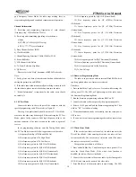
Chapter 3 Circuit Description
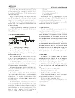
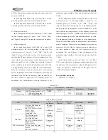
3.1 Frequency Configuration
RF
AMP
5T
TX/RX SW
5T
5R
RF
AMP
5C
BUFFER
RXVCO
TXVCO
MODE
RIPPLE
FILTER
5C
BUFFER
PLL IC
DATA FROM MCU
CLK FROM MCU
LE FROM MCU
PS FROM MCU
LOCK TO MCU
TCXO
12.8MHz
QT/DQT FROM MCU
CENTER FREQUENCY ADJUST FROM MCU
5C
5C
MIXER
5R
IF
AMP
5R
5C
12.8MHz TO
51.2MHz
DET COLL
51.65MHz
+/- 15KHz
+/- 7.5KHz
450KHz
NOISE
AMP
TA31136
NOISE DET
BUSY SIGNEL TO MCU
5R
Figure 3.1 Frequency Configuration
The reference frequency of the frequency synthesizer is
provided by crystal oscillator X4 (TCXO, 12.8MHz). The receiver
adopts double mixing. The first IF is 51.65MHz and the second IF
is 450kHz. The first local oscillator signal of the receiver is
generated by the frequency synthesizer. The second local
oscillator signal adopts the fourth harmonics (51.2MHz) of the
crystal oscillator X4 (TCXO, 12.8MHz). Transmitter signal is
directly produced by the frequency synthesizer.
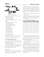
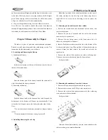
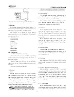
3.2 Principle of Receiver (RX)
Figure 3.2 Principle of Receiver
Front end
The signal coming from the antenna passes through the
RX/TX switch circuit (D1, D2, D4 and D5), and passes through a
BPF comprises of C37, C227, L8, L15, C70, C126, D30, C218,
L9, C230, C128, D26, C217, L10, C229, C127 and D24 to
remove unwanted out-of-band signal, and is sent to the low noise
amplifier (LNA) consists of Q20 and its peripheral components to
be amplified.
Output signal from the LNA passes through a BPF comprises
of L7, C228, C47, D23, C219, L6, C182, C124, D22, C216, L5,
C132, C32 and D21 and goes to the first mixer (Q19).
PWM wave is output from pin 12 of the MCU. The wave is
filtered and rectified into adjustable voltage, which can control the
center frequency of the band pass filter through changing capacity
of the varactor diodes (D21, D22, D23, D24, D26 and D30).
First mixer
The received signal from LNA is mixed with the first local
oscillator signal from the frequency synthesizer to produce the
first IF signal (51.65MHz). Then the first IF signal passes through
crystal filter (XF1 and XF2) to remove the adjacent channel signal
and signal outside the adjacent channel.
IF circuit
The first IF signal from the crystal filter is amplified by the
first IF amplifier (Q21), and is sent to the IF processing IC (IC5,
TA31136).
IF IC consists of second mixer, second local oscillator, IF
amplifier, limiter, discriminator, and noise amplifier.
The 12.8MHz frequency produced by TCXO (X4) is
multiple-amplified and then the fourth harmonics (51.2MHz) is
adopted as the second local oscillator signal source. The second
local oscillator signal (51. 2MHz) is mixed with the first IF signal
(51.65MHz) in IC5 to generate the second IF (450kHz). And then
the second IF signal is amplified and limited in IC5, filtered by the
ceramic filter (CF1, 450kHz), and demodulated in IC5 to output
audio signal.
Figure 3.3 IF System


