background image

DPC-885

5

CIRCUIT DESCRIPTION

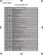
Pin No.

Name

I/O

Function

91

LINE

I

Line out detection terminal

92

HOLD

I

HOLD switch on/off

93

LD

O

Laser diode output terminal

94

LIDSW

I

Cover open detection switch

95

XWIH

O

Write permission signal output for RL5C356

96

XEMP

I

Read prohibition signal input for RL5C356

97

XWRE

I

Write prohibition signal input for RL5C356

98

XQOK

O

CD sub code Q OK signal output for RL5C356

99

XLT

O

LATCH output to RL5C356

100

SQSO

I

CDQ code data input from CXD 3009Q

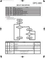
2. Test Mode

2-1 Setting the test mode

This model can be set to the test mode by shorting
the test-land of the X32 board.

START

Turn on lid

switch

Is test land

shorted?

Test mode

processing

Is key pushed?

Track No. "01"

is displayed.

TEST MODE

YES

NO

NO

See following table.

Normal operation

No.

Mode

Key Name

Function

TRACK No. display

1

05

PLAY/PAUSE

(

6

)

1. Focus servo.....................................................................................................ON 
2. Tracking servo.................................................................................................ON 
3. Feed servo ......................................................................................................ON
Absolute time at position of limit SW is displayed in time area, then play is started.

05

After 1, 2 and 3 are
finished, track No.
played currently and its
play time are indicated.

2

03

UP

(

¢

)

1. Focus servo.....................................................................................................ON 
2. Tracking servo...............................................................................................OFF 
3. Feed servo ....................................................................................................OFF

03

3

01

STOP

(

7

)

1. Focus servo...................................................................................................OFF 
2. Tracking servo...............................................................................................OFF 
3. Feed servo ....................................................................................................OFF 

✜ 

Test mode can be can celled while pressing the STOP (

7

) Key in 01 mode.

01

4

While pressing the
P. MODE/SEARCH Key, 
turn the AC ON

All LCD is turned ON for 2 seconds. 

ó

All LCD is turned OFF for 2 seconds. 

ó

Returned to normal mode.

2-2 Key and functions avild in test mode

COVER/CIR/EXP-INT 


98.4.24 

2:57 

PM 

 y [ W  

5

Summary of Contents for DPC-885

Page 1: ... V Battery life continuous repeat playback Figures inside parentheses are the values when D A S C is ON Commercially available alkaline batteries LR6 AA x 2 Approx 17 5 15 hours Rechargeable batteries NB 130 x 2 Approx 9 0 8 0 hours Dimensions W x H x D 132mm x 32mm x 153mm 5 3 16 x 1 1 4 x 6 Weight net 270 g 9 5 oz SPECIFICATIONS 1 KENWOOD follows a policy of continuous advancements in developmen...

Page 2: ...7 05 Remote control 1 A70 1163 05 MX A70 1164 05 KPET AC adapter 1 W08 0658 05 E W08 0659 05 T W08 0660 05 X W08 0667 05 M W09 1251 05 KP Carrying case 1 W01 0939 05 SPECIFICATIONS Top cover CONTENTS ACCESSORIES 2 CIRCUIT DESCRIPTION 3 ADJUSTMENT 6 PC BOARD 7 SCHEMATIC DIAGRAM 9 EXPLODED VIEW 15 PARTS LIST 17 Accessories CONTENTS COVER CIR EXP INT 98 4 242 57PM y W 2 ...

Page 3: ...NDICATOR AUTO POWER OFF IC3 28Pin UNIT KEYS 1 UNIT KEYS 2 LCD H P REMOCON KEYS BATTERY VOLTAGE IC3 29Pin IC3 33Pin IC3 31pin 32Pin CD ASP CD DSP 1bitDAC uPD78063GF 138 LCD A D KEY LCD KSM542DBA CXA1982Q CXD3009Q RL5C356 8M D RAM u COM COM X 4 SEG X 13 A D KEY DISPLAY FOK IC 6 IC 2 IC 1 IC 3 AUDIO LINE 1 2 3 4 5 6 7 TRAVERSE UNIT CONTROL REMOCON SENSOR AUDIO OUTPUT SHOCK PROOF MECHA DRIVER LINE 1 M...

Page 4: ...hargeable battery 33 HP KEY I HP Key input terminal for display 34 NC Not used 35 ADON O A D converter on off 36 AVDD Analog power supply for A D converter 37 AVREF Reference voltage input for A D converter 38 SLTSW I Start limit switch of pickup 39 DCDC ON O DC DC converter control H ON L OFF 40 VSS GND 41 ADPT I Adaptor detection H OFF L ON 42 CHRGOK I Voltage level of rechargeable battery detec...

Page 5: ...orted Test mode processing Is key pushed Track No 01 is displayed TEST MODE YES NO NO See following table Normal operation No Mode Key Name Function TRACK No display 1 05 PLAY PAUSE 6 1 Focus servo ON 2 Tracking servo ON 3 Feed servo ON Absolute time at position of limit SW is displayed in time area then play is started 05 After 1 2 and 3 are finished track No played currently and its play time ar...

Page 6: ... or AC voltmeters Connect a LPF between Check land TE1 and TE2 to which connect an oscilloscope or AC voltmeters Connect an oscilloscope as follows CH1 RF Check land RF CH2 TE1 PLAYER SETTING Press the PLAY key Confirm that the display is 05 Press the PLAY key Confirm that the display is 05 Press the PLAY key Confirm that the display is 05 ALIGNMENT POINT TE BALANCE VR5 FOCUS GAIN VR4 TRACKING GAI...

Page 7: ...ponent side view PC BOARD Foil side view 7 8 X32 3350 01 M2 X32 3350 10 KPET X32 3350 21 MX X32 3350 01 M2 X32 3350 10 KPET X32 3350 21 MX Refer to the schematic diagram for the value of resistors and capacitors DPC 885 K PCB SD 98 3 204 43PM y W 1 ...

Page 8: ...5 6 7 9 7 5 13 3 FCS FCS TRK TRK AL F VC VCC LD GND VR PD E PD1 PD2 1 3 2 5 4 15 14 13 12 11 10 9 8 7 6 VR3 22K 10K R127 10K R130 R131 24K R128 4 7 C126 47u4 R132 24K C116 0 047 C117 0 01 C118 4700P C119 0 01 R114 2 2K R115 4 7K R113 22K C121 33P R137 100K 14 12 13 11 10 R121 100K C115 0 01 C26 22u4 C113 0 01 R110 C112 1 R109 220K VR4 22K C108 R104 C107 0 01 R103 510K C106 C104 0 1 R138 R107 C105 ...

Page 9: ...VO C41 0 1 C18 100u4 33K R24 L2 25 27 29 31 10K R27 C33 0 01 1 3 2 IC11 L3 7 8 6 5 5 31 D0 A3 10 9 44 VCC 43 A2 470K R315 R19 220P 470uH L1 10u10 C35 1000P C39 1000P 1000P C37 OP C36 22u10 C20 22u6 3 C43 1000P 1000P C31 PREGND 7 9 5 3 C8 0 01 R18 13K C44 3 VO EXT 4 2 VDD 1 VSS CE 5 R22 220 C17 100u10 C19 100u6 3 R17 10K 44 95 21 44 VCC 1 XQOK 2 XWRE 3 XEMP 4 XWIH 5 C176 6 CHDT 7 EBLK 8 CLK 9 GND 1...

Page 10: ... 30 27 C434 4 7u4 C433 4 7u4 R431 680 DATA Rch Lch VREF 1000P 1000P C308 1000P R336 10 R335 10 GND KEY COM0 COM2 COM3 S0 S1 S2 S3 S4 S5 S9 S6 S7 S8 S10 S11 S12 S13 KEY1 KEY2 S14 GND 0 01 C309 C312 0 1 GND SWITCH B COM1 S10 S9 S8 S7 S6 S5 S4 S3 S2 S1 S0 COM3 COM2 COM1 COM0 GND KEY2 KEY1 S14 S13 S12 S11 R401 22K C404 1200P R404 8 2K C403 1200P R403 8 2K 47u4 C420 16 PWSW MUTE 1 15 INA OUTA 2 14 INC ...

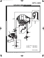
Page 11: ... AA M2x2 5 BLK AB M2x8 AC M1 7x1 8 N09 3425 08 N09 3424 08 N39 1718 46 1 4 2 5 3 808 809 811 810 1 2 3 A B Parts with exploded view numbers larger than 700 are not supplied 15 EXPLODED VIEW MECHANISM COVER CIR EXP INT 98 4 242 57PM y W 7 ...

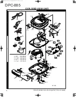
Page 12: ... N09 2866 05 N09 3399 05 N09 2893 05 N09 3397 05 N09 3369 05 608 609 647 602 612 601 625 646 635 657 655 642 643 643 621 633 614 629 651 603 636 626 638 634 652 656 604 660 620 658 634 632 645 616 644 637 P1 P2 P3 J 4 LINE OUT 628 627 1 2 3 C D Parts with exploded view numbers larger than 700 are not supplied 16 EXPLODED VIEW UNIT COVER CIR EXP INT 98 4 242 57PM y W 8 ...

Page 13: ...GB1H221K CHIP C 220PF K C104 CK73GB1C104K CHIP C 0 10UF K C105 C92 0507 05 CHIP TAN 4 7UF 6 3WV C106 CK73GB1C333K CHIP C 0 033UF K C107 CK73GB1E103K CHIP C 0 010UF K C108 CK73GB1E223K CHIP C 0 022UF K C110 CK73GB1H221K CHIP C 220PF K C112 CK73FF1C105Z CHIP C 1 0UF Z C113 CK73GB1E103K CHIP C 0 010UF K C114 C92 0619 05 CHIP TAN 47UF 4WV C115 CK73GB1E103K CHIP C 0 010UF K C116 CK73GB1C473K CHIP C 0 0...

Page 14: ... CHIP R 15K J 1 16W R111 RK73GB1J513J CHIP R 51K J 1 16W R112 RK73GB1J224J CHIP R 220K J 1 16W R113 RK73GB1J223J CHIP R 22K J 1 16W R114 RK73GB1J222J CHIP R 2 2K J 1 16W R115 RK73GB1J472J CHIP R 4 7K J 1 16W R116 RK73GB1J162J CHIP R 1 6K J 1 16W R117 RK73GB1J394J CHIP R 390K J 1 16W R118 RK73GB1J184J CHIP R 180K J 1 16W R119 RK73GB1J223J CHIP R 22K J 1 16W R120 RK73GB1J105J CHIP R 1 0M J 1 16W R12...

Page 15: ...D29 DA204U DIODE IC1 CXA1982Q ANALOGUE IC IC2 CXD3009Q MOS IC IC3 UPD78063GF 138 MI COM IC IC4 LA4800V ANALOGUE IC IC5 BH6504K MOS IC IC6 RL5C356 MOS IC IC7 8 MN41V4400TT 07 MEMORY IC IC7 8 MN41V4400TT 08 MEMORY IC IC9 NJM2904M IC OP AMP X2 IC10 NJM2903M IC COMPARATOR X2 R124 RK73GB1J103J CHIP R 10K J 1 16W R125 RK73GB1J123J CHIP R 12K J 1 16W R126 127 RK73GB1J103J CHIP R 10K J 1 16W R128 RK73GB1J...

Page 16: ...hout Parts No are not supplied Les articles non mentionnes dans le Parts No ne sont pas fournis Teile ohne Parts No werden nicht geliefert Ref No Add ress New Parts Description Desti nation Re marks Parts No L Scandinavia K USA P Canada R Mexico M2 Hongkong Y PX Far East Hawaii T Europe E Europe G Germany Y AAFES Europe X Australia M Other Areas indicates safety critical components IC11 RN5RG29AA ...

Reviews: