background image

Summary of Contents for 171

Page 1: ...Instruction Manual Model 171 Digital Multimeter 01997 Keithley Instruments Inc Cleveland Ohio U S A...

Page 2: ...KEITHLEY INSTRUMENTS 1 N C INSTRUCTION MANUAL MODEL 171 DIGITAL MULTIMETER...

Page 3: ...r Card 20 4 5 Model 1007 Dual Rack Mounring Kit 20 4 6 Model 2000 Rack Mounting Kit 21 5 Maintenance 5 1 General 27 5 2 Required Test Equipme 22 5 3 Performance Checks 22 5 4 Adjustment and C libratio...

Page 4: ...17 16 A to D Converter Block Diagram 19 17 Model 1007 Dual Rack Mounting Kit Exploded View 21 18 Model 2000 Rack Mounting Kit Exploded View 21 19 Cutaway View Showing PC Board Locations 23 20 calibrat...

Page 5: ...f0 003 Of range 0 008 0 100 d range l C INPUT IMPEDhNCE i Ml shunted by a proxi ately 100 pl SETTLING TIM Less than 3 seconds except for ac superimposed on dc MAXIMUMSAFE INPUT 1000 volts dc or rms ac...

Page 6: ...I MODEL171 SECTION 1 GENERAL DESCRIPTION 773...

Page 7: ...raph Turns on instrument power 2 3a sets dc voltage functian 2 3c set 5 ac voltage function 2 3c sets ohms function 2 3c Sets dc ampere function 2 3c sets ac ampere function 2 3c sets instrument sensi...

Page 8: ...ampere OUTPUT BCD OUTP T LINE Input Analog output 1v for full range Provides digital outputs with Model 1712 installed as shown connector not provided without Model 1712 receptacle mates with 3 wire...

Page 9: ...ng The circuit ground to chassis ground isolation is greater than 100 megohms shunted by less than 0 02 microfarad Circuit ground may be floated up to 2500 volts With respect to chassis ground in a11...

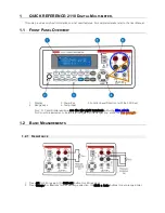
Page 10: ...I I I 2 3 4 5 mYI...

Page 11: ...f the 1712 These stages utilize open collector output transis tars thaf may be operated at c mon DTL and TT olt age levels as well as others up LO f12 volts I addition the Model 1712 has ar exeensive...

Page 12: ...rs and mating panel mount co nector 773 OPERATION Ribbon type 57 30500 Keichley cs 220 The optional Model 4405 Terminal BOX and Model 1801 output Cable see Table 2 6 are i al interfacing accessories F...

Page 13: ...lines of the particular instrument of inter est when not using rhe strobe feature of the 1712 keep all strobe lines closed to common ground 5 Hold The Hold remote control by closure retains the result...

Page 14: ...31 32 33 34 35 36 37 38 39 40 41 42 43 44 45 46 47 48 49 50 C m 0 GNU Clock see Para Z 911 Count interval see Para 2 9e2 G see Parh 9f3 see Para 9f3 Flag Logic 1 SO Lange Availabi Function 1 see T xbi...

Page 15: ...ur BCD bits representing the thousands digit of a reading e Strobe Data 83 Closure of this line enables simultaneous conduction of data from pin numbers 9 10 11 and 12 the four BCD bies representing t...

Page 16: ...773...

Page 17: ...POLARITY BLANKING r T _ _______ _ __ 1 s i 1 I I i I I I I I I I ij L A OHMS OHMS 1 5 CONVERTER 1 SLCS L AC DC I h CONVERTER DEMODULATOR ANALOG r OUTPUT k i i _ kWUTLo il...

Page 18: ...SECTION 3 CIRCUIT DESCRIPTION 1 1 v I 10 In 4 99k I 499 k 100 100 mv 4 99k Y 39 2k 10 1 v 4 99k 0 1 I 10 4 99lc 0 1 100 4 99kl 0 I 1000 4 99kcn 0 1...

Page 19: ...vision which results in a chopping frequency of 227 27 Hz U ffU Amplifier This circuir provides drive signals for the switching transistors in the modu lator and demodulator circuits Transisrars 9508...

Page 20: ...Range Shunt it Volt sensitivity ndjustmc 1 Llri 100 kil 100 rn 10 A 10 a 100 m 1 00 llii I k i 100 rn ImA 100 12 100 1 10 mh 1 2 100 100 IA I I 100 3 1000 IVA 0 1 1 JO a...

Page 21: ...e 2 period i e the Zeroing Period d Integrator located on R 301 e zero crossing Detecmr located on PC 301 f Buffer Storage Register located on K 299 4 Circuitry a Clock An oscillator composed of integ...

Page 22: ...ircuit controls the overrange 1 whenever the full range exceeds 9 9 9 9 1 Numerical Readouts The four numerical readouts 204 203 202 and 201 are riven by Decoder Driver modules Q 4219 QA216 QA213 and...

Page 23: ......

Page 24: ...I 773...

Page 25: ...SECTION 4 ACCESSORIES...

Page 26: ...CI l 1 FIC rn 17 f fodcl 1007 Dual Rack Mounting Kit Exploded View FIG RE 18 Model 2000 Single Rack Mounting Kit Exploded View 773...

Page 27: ...w note that if the ambient temperature is not at 25 C the temperature coefficients listed in the various Accuracy Check Tabl es 5 2 5 3 5 4 5 5 5 6 should be used to calculate the allowed rending tole...

Page 28: ...rminals HI and LO Apply a 60 Hz 50 v t p p sine wave f the CASE and HI input of the 171 using Oscillator F c Apply a 60 Hz 9 5 volt p p sine wave t the input of the 171 using Oscillator F trans former...

Page 29: ...y Reading TOlera Ce CO ZffiCie t 1OrnV 0 0035 1omv 10 000m i4 digits f0 4 digit Y loom 0 0035 loom 100 00m f3 digits iO 4 digit C 1 io o035 1 1 0000 i3 digits i0 4 digit Y 10 v iO O032 10 10 000 v r3...

Page 30: ...14 40HP200HZ 1UA 1 0000uA 160 digits 5 digits C lOuA i 0 14 40Hz 10kHz lOuA 10 000UA 160 digits 5 digits Y lOO lA iO 14 40 z 10kHz 1OOUA 100 00 A f160 digits 5 digits Y l lA 0 14 40Hz 10kHz lll A 1 0...

Page 31: ...Figure 21 oo the in tegrator board R 301 and input LO If a reading of 5 i250m is not obtained proceed with troubleshooting and repair 2 15 Volt Supply Measure the 15 supply between 15V P 2 see Figure...

Page 32: ...referencing Figures 20 and 21 4 IO loo 1000 Calibriltio I open nccesa cover c see iigure 2 b Using Voltage Source A supply inpur LIP the 171 with appropriate RANGE switch settings s specified in Tabl...

Page 33: ...essary ad just Par 111 102 see Figures 20 and 21 h AC olfage Calibration 1 pen ACCeSS cover c see Figure 20 2 sing Voltage sourm I eat is rhe H P 145A or H P 745 H P 74 t supply inpurs co the 171 with...

Page 34: ...f 150 r 0 0 t OOv 0 0 f 125 0 0 L105U 0 0 t 105 0 0 1125 v 0 0 150 1 0 0 t200 v K520 NONE TABLE 5 9 htegrator Reference dc Voltage Calibration Test VOltage Display Adjust NO source D eexling Pot 1 1...

Page 35: ...100 00 01 K LO 000 i 005 K l OO O 0005K lOOO b o K 1 0000 0004E 10 001 I I M 100 00 2 0 M 1000 0 25 Mi lO O I O ERL hD 30...

Page 36: ...YOKE 1 0 400 HZ 1 0000 i 0 27 NONE 1 0 v 40 HZ 1 0000 0023 NUKE 100 rn 40 HZ 100 00 2 44 NONE 100 m 400 HZ 100 00 f 52 NONE 100 Ill 10 kHZ 100 00 52 NONE 1 0 In 10 kHZ 1 00 2 I6 v NONE 100 In 100 kHz...

Page 37: ...I MAINTENANCE ACCESS COVER B I 32 773...

Page 38: ...I RlllO t 1 R1102 TR1007 yR1003 R1004 TP 16 TP 15...

Page 39: ...MAINTENANCE MODEL 171 773...

Page 40: ..._ I 8101 II0 ol l q Yq J I O d hl IIll 0 P...

Page 41: ...I IIIIP 0 06...

Page 42: ...MODEL 171 FIGURE 26 Component Layout Integrator Board PC 301 MAINTENANCE 773 37...

Page 43: ...MAINTENANCE I FIGURE 27 Component Layout Tube Board PC 299 I 38 MODEL 171 773...

Page 44: ...MODEL 171 MAINTENANCE FIGURE 28a Component Layout Optional Digital Output PC 275a I _ __ FIGURE 28b Component Layout Optional Digital Output PC 275b 773 39...

Page 45: ...SECTION 6 REPLACEABLE PARTS...

Page 46: ...g location of electrical and mechanical parts to a particular printed circuit assembly I assemblies Reference is made to the manual pages replaceable parts list that contain all parts of a particular...

Page 47: ...REPLACEABLE I ARTS MODEL 171 773 42...

Page 48: ...4713 MC858P MISCELlANEO S Mfr Mfr I...

Page 49: ...p camp camp camp camp camp camp Camp Camp camp camp camp camp camp camp camp camp camp camp camp CB103 10 CB103 10 CB103 10 CR103 10 CR103 10 CB103 10 C 1 03 10 CB103 10 clJ103 10 CB103 10 CB103 10 C1...

Page 50: ...7 D203 Germanium 15238 IN87 RF 39 27 204 Germanium 15238 iN87 RF 39 27 D205 cermanium 15238 lN87 w 39 27 1NTEGRATEDCIRCUITS QA201 CL 91Flip Flap ll pin DIP QA202 Dual Flip Flap 14 pin DIP QA203 Positi...

Page 51: ...0 K211 R212 R213 R214 R215 K216 R217 1 a 22 kn 100 kc2 3 3 kn 3 3 kfi 470 n 10 kn 10 in 10 krl 10 kR 220 n 100 IdI 80 6 kR 47 kn 7 87 kR kR o n IO l 4 w IO l 4 w IO 1 lO l 4 w IO l 4 lO l 4 w l l 2 w...

Page 52: ...6 DD 050 C64 5P TSD5 5 LO A C205 LOOM ID 050 C64 5F TD2 20 106 20 CL79 ION 26 26 26 26 _ 14752 100 1000 loo0 __ 1000 50 15 15 Y 1000 15 000 __ 20 15 20 1000 500 500 500 v 97419 71590 56289 71590 14752...

Page 53: ...e NOR Gates I4 pin DIP SI 12916 IC 2 26 LM311 IC 29 26 SN7401 TC 47 26 SN7402N IC 32 26 SN7404N IC 33 26 26 26 26 26 26 26 26 26 26 26 26 26 26 26 26 26 26 26 26 26 26 26 26 26 26 26 26 26 26 26 26 26...

Page 54: ...O CB Lo 10 lx 47R 10 C t T O CB 47L 10 CB 472 10 C hT O CEA T O 1176 Lk 26 R88 392k 26 Ka8 LOOk 26 R88 LM 26 K88 301k 26 R88 3Oik 26 R76 47 26 K76 2 2k 26 R76 4 7 26 K76 4 7 26 K88 LM 26 R76 4 7 26 R...

Page 55: ...25 CerD 56289 XAS S10 C22 OlM ii cerLl 56289 XXS SIO C22 OlM 25 CerF 72982 8131 050 651 474M C237 47M 25 07263 lN4607 RF 41 25 15238 IN87 RF 39 25 15238 lN87 RP 39 25 01295 lN645 RF 14 25 01295 IN914...

Page 56: ...80 IO R76 6 R417 4 02G 1 l S w MtF 75042 CO T O K88 4 02K R418 10 KG IO 1 4w camp 01121 CB103 10 R76 10K 25 25 25 Q401 Q402 0403 75042 CEA T O 75042 CM T O 01121 CB221 10 TRANSISTORS Mfr Mfr Keiehley...

Page 57: ...NO Ref QA501 Operational Amplifier 8 p Mini DIP 12040 SL12917 IC 24 23 QA502 Operational Amplifier pin Mint DIP 12040 LM741CN n 42 23 QA503 Operational Amplifier B pin Mlnl DIP 12040 SL12917 K 24 23...

Page 58: ...met ar camp NCF MtF COSp ccrmct ar MCF coinp MU camp MtF cermet var MC fit3 cermet ar cermet aI Fixed Fixed 75042 011 21 01121 01121 1121 01121 75042 75042 01121 75042 75042 01121 73138 _ _ 0164 73118...

Page 59: ...C902 see MOTHERBOARD 900 SERIES 97419 71590 MZW R C143 047M CPR 3300 T C138 0033M 831 Z5 O 222M CZZ 0022M 871 Z5 O 103M CZZ OlM TDl ZO 226 26 C179 22M W 20 474 20 C179 47M WI 035 224 20 CL79 22M m 391...

Page 60: ...906 R907 R908 XL 909 R910 989kn 25 kc2 Not USed 500 5 kn 5 kn 1 2 w MS 03888 PME 80 989K lO 0 75 w cermet var 73138 89P 25K ___ lO 0 75 w cermet var 73138 89P 500 lO 0 75 w C snlEL var 73138 89s5K lO...

Page 61: ...21 73138 01121 75042 75042 CB154 10 R76 150K 27 89P 5K RP89 5K 27 CB105 10 R76 1M 27 C T O R88 4 75K 27 CFA T O R88 4 75K 27 R1106 6 98 kfl 1 l 8 w RllOJ 28 7 kn l l 8 W R1108 28 7 k0 l l 8 W RllOV 13...

Page 62: ...pF 1000 CUD 71590 C716 C717 C718 CT19 47 pF 1000 CerD 71590 47 pF 1000 ceri3 71590 047 UF 600 v MP0ly 97419 47 UF 600 V MPdy 97419 C901 See FRONT PANEL 900 SERIES C902 l pF 1200 m 221 TD22010620 TD220...

Page 63: ...Buteon Rear Guarded section CS 251 22 CS 236 22 3901 3902 51202 1203 71785 71785 71785 71785 79727 _ _ 80164 80164 2521830240 2521830240 CS 260 22 CS 260 22 CS 242 22 CS 242 22 2522230160 2522230160...

Page 64: ...Power TO 66 Case 02735 40312 z 54 q703 Silicon NPN TO 92 case 04713 2N5551 U 67 q704 Silicon NPN TO 92 Case 04713 2135551 X 67 Q705 Silicon NPN TO 92 case 04713 2N5551 X 67 Q706 Silicon NPN TO 92 case...

Page 65: ...SERIES Mfr Lbsig LM309K Q 4701 T701 F701 Integrated circuit Voltage Regulator TO 3 case 12040 Transformer Power 80164 Fuse 3AC 125 Volt Slo 310 l 2 amp for 105 125 V Ooeracion 71400 IC 34 m 141 F 4 N...

Page 66: ...er for XEAK PANEL ruse F7Ol I Fii 11 Fuse itolder for MOTHERBOARD Fuse F 901 2 Fii 12 Push Buttons Plastic for 5903 s907 Front section 5 i B 3 Push B etons for S903 S907 Rear Section Guarded 5 21883 S...

Page 67: ...REPLKEAULE PARTS t lo 66 c KEITHLEY PART NO TG 41 KEITHLEY PART NO TG 51 KEITHLEY PART NO TG 42 KEITHLEY PART NO TG 52 TO 72 2 ml m YIEW NlnmCTIoN 62 773...

Page 68: ...KEITHLEY PART NO TG 76 Q j R 110 t _ KEITHLEY PART NO IC 2 63...

Page 69: ...I EITHLEY PART NO IC 2 24 fzJ TO 99 KEITHLEY PART NO IC 25 L 64...

Page 70: ...MODEL 171 KEITHLEY PART NO IC 31 EITHLEY PART NO IC 33 IC 80 IC 81 I IKEITHLEY PART NO IC 32 KEITHLEY PART NO IC 35 773...

Page 71: ...I I I EITHLEY PART NO IC 36 KEITHLEY PART NO IC 38 KEITHLEY PART NO IC 37 I I I I I I I 11 if I i I ii I EITHLEY PART NO IC 39 66...

Page 72: ...I MODEL 111 KEPLACEABLE PAKTS KEITHLEY PART NO IC 43 JEDEC TO 116 KEITHLEY PART NO IC 47 v 8 a il KEITHLEY PART NO IC 48 67...

Page 73: ...ille N J 08093 Gulton Industries Inc Alkaline Battery Div bleeuctlen N J Burgess Battery co Div of Clevife Carp Freeport 111 Burndy Corp Norwalk Corm 06852 CTS of Asheville Inc Skyland N C 28776 IRC I...

Page 74: ...ueller Electric co Cleveland Ohio 44114 Resistance Produces Co Harrisburgh Pa 17104 c ontinenta1 wire Electronics Corp Philadelphia Pa 19144 Keithley Instrumenes Inc Cleveland Ohio 44139 BO r S 1 C Ri...

Page 75: ...1 RI1 L FZ t c r 003 1 1 i I...

Page 76: ...5...

Page 77: ...IY I I...

Page 78: ...I c j...

Page 79: ......

Page 80: ...i 5 ii c s ___...

Page 81: ...I t 0...

Page 82: ......

Page 83: ...r...

Page 84: ...fh I J 1 I n I...

Page 85: ...r J I _...

Page 86: ...4...

Page 87: ......

Page 88: ......

Page 89: ......

Page 90: ...ion Equipment at the factory 0 Certificate of Compliance 3 DESCRIPTION OF PROBLEM Include a block diagram of instruments connected in system Recorder charts or other data would be helpful Is problem c...

Page 91: ...l into the follow ing categories 1 Report of Calibration Certified Traceable to the National Bureau of standards 2 Calibration Report 3 Certificate of Compliance 4 Recalibration All calibration and ce...

Reviews: