GB - 21
6. Functional Description
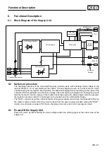
6.1 Block Diagram of the Supply Unit
6.2 Switch-on procedure
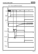
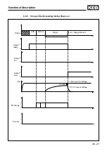
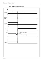
The charging procedure of the connected frequency inverters starts with releasing mains voltage to the
input terminals L1, l2, L3 and starting of the control. The pre-charging occurs via a current source, which
enables loading of very high DC link capacities. The obtained charging time is depending on the value of the
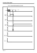
connected DC link capacities and the mains voltage. After executed pre-charging and checking the ground
fault free at the DC bus the release of the thyristor block takes place. No phase angle control is executed,
the thyristors are driven with 0° control angle, so the behaviour is like a B6-rectifier bridge.
The "RUN" - signal is set at the control terminals of the power supply unit and can be processed further by
the master control. A load current may only be taken from the power supply unit after setting the "RUN" -
signal, since otherwise a power off of the pre-charging unit occurs and an error message is output.
6.3 Power-Off the Supply Unit
Power-off occurs by disconnecting the mains voltage and/or the starting signal at the control card at the
supply unit.
L1
L2
L3
3
3
24 VDC
560 VDC
PA
PB
+
-
6
Functional Description
Current measurement
B6 Charge Rectifier
Current supply
Electronics
Heat sink
temperature
Ready for ope-
ration
Pre-warning
Main thyristors
GTR7
(Option)
DC-fuses
(Option)

