background image

16

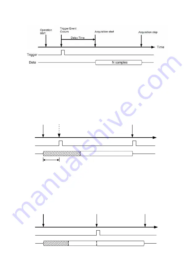
Figure 3-6: Delayed Trigger Mode Acquisition

3�4�3    Pre-Trigger Mode

Collects data before the trigger event, starting once specified function calls are executed to begin the 

pre-trigger operation, and stopping when the trigger event occurs. If the trigger event occurs after 

the specified amount of data has been acquired, the system stores  only  data  preceding  the  trigger  

event  by  a  specified amount, as follows.

Time

Operation start

Acquisition start

Trigger

Data

Trigger Event Occurs

Acquisition stop

Data transfer to system begins

N samples

X samples have been acquired

before trigger occurs, where X<N

Trigger signals occuring before the specified 

amount of data has been acquired are ignored

Figure 3-7: Pre-Trigger Mode Acquisition

3�4�4    Middle Trigger Mode

Collects data before and after the trigger event, with the amount to be collected set individually (M 

and N samples), as follows

Time

Operation start

Acquisition start

Trigger

Data

Acquisition stop

Data transfer to system begins

N samples

M samples

Trigger event occurs

Figure 3-8: Middle Trigger Mode Acquisition

Summary of Contents for PCIe-69852

Page 1: ...01 PXIe 69852 2 CH 14 Bit 200 MS s Digitizer User s Manual Manual Rev 1 00 Revision Date Jul 16 2016...

Page 2: ...minor physical injury component damage data loss and or program corruption when trying to complete a task Information to prevent serious physical injury component damage data loss and or program corr...

Page 3: ...on 11 3 2 2 Input Range and Data Format 11 3 2 3 DMA Data Transfer 12 3 3 Trigger Source and Trigger Modes 13 3 3 1 Software Trigger 14 3 3 2 External Digital Trigger 14 3 3 3 PXI STAR Trigger 14 3 3...

Page 4: ...DC Timing Control 19 3 6 1 Timebase Architecture 19 3 6 2 Basic Acquisition Timing 19 3 7 Synchronizing Multiple Modules 22 Appendix A Calibration 23 A 1 Calibration Constant 23 A 2 Auto Calibration 2...

Page 5: ...1 3 Digital Trigger Input 4 Table 1 4 Digital Trigger Output 5 Table 1 5 PXIe 69852 I O Array Legend 8 Table 3 1 Input Range and Data Format 12 Table 3 2 Input Range FSR and FSR Values 12 Table 3 3 In...

Page 6: ...Trigger Architecture of the PXIe 69852 13 Figure 3 4 External Digital Trigger 14 Figure 3 5 Post Trigger Acquisition 15 Figure 3 6 Delayed Trigger Mode Acquisition 16 Figure 3 7 Pre Trigger Mode Acqui...

Page 7: ...auto calibrated with an onboard reference circuit calibrating offset and acquiring analog input errors Following auto calibration the calibration constant is stored in EEPROM such that these values c...

Page 8: ...sine wave 7Vrms with Peaks 10V 50 Input impedance 50 or 1M software selectable Offset error 1 mV Gain error 0 65 SNR 56dB 1M 0 2 V 62dB 1M 2V 62dB 1M 10V 60dB 50 0 2V 62dB 50 2V THD 73dB 1M 0 2V 69dB...

Page 9: ...7 6 5 4 3 2 1 0 Bandwidth Frequency Hz Magnitude dB Figure 1 1 Analog Input Channel Bandwidth 0 2 Vpp 0 1M 0 3M 1M 3M 10M 30M 100M 300M 9 8 7 6 5 4 3 2 1 0 Bandwidth Frequency Hz Magnitude dB Figure 1...

Page 10: ...ebase 1 3 3 Triggers Trigger Source Mode Trigger source Software external digital trigger analog trigger PXI_STAR PXI_trigger bus 0 7 and PXIe_DSTARB Trigger mode Post trigger delay trigger pre trigge...

Page 11: ...idity 5 95 non condensing Storage Temperature 20 C 80 C Relative humidity 5 95 non condensing Calibration Onboard reference 5 V and 2 5 V Temperature coefficient 3 0 ppm C Warm up time 15 minutes Powe...

Page 12: ...and DLL for Windows XP 7 8 DLL is binary compatible across Windows XP 7 8 This means all applications developed with WD DASK are compatible with these Windows operating systems The development enviro...

Page 13: ...7 The PXIe 69852 I O array is labeled to indicate connectivity as shown Figure 1 4 PXIe 69852 I O Array...

Page 14: ...ck to digitizer Ext Digital Trigger Input TRG IN External digital trigger input receiving trigger signal from external instrument and initiating acquisition Trigger Output TRG OUT Trigger output in wh...

Page 15: ...be easily damaged by static electricity The module must be handled on a grounded anti static mat The operator must wear an anti static wristband grounded at the same point as the anti static mat Inspe...

Page 16: ...ith the module guide in the PXIe chassis 3 Slide the module into the chassis until resistance is felt from the PXIe connector 4 Push the ejector latch upwards and fully insert the module into the chas...

Page 17: ...tes with equivalent 50 or 1 M input impedance selected by software The 14 bit ADC provides not only accurate DC performance but also high signal to noise ratio and high spurious free dynamic range in...

Page 18: ...A transfer the hardware temporarily stores acquired data in the onboard AD Data FIFO and then transfers the data to a user defined DMA buffer in the computer Using a high level programming library for...

Page 19: ...dress Transfer Size Next Descriptor Figure 3 2 Linked List of PCI Address DMA Descriptors 3 3 Trigger Source and Trigger Modes This section details PXIe 69852 triggering operations Figure 3 3 Trigger...

Page 20: ...l Digital Trigger 3 3 3 PXI STAR Trigger When PXI STAR is selected as the trigger source the PXIe 69852 accepts a TTL compatible digital signal as a trigger signal Triggering occurs when a rising edge...

Page 21: ...able from 50ns to 10 s via software 3 4 Trigger Modes Trigger modes applied to trigger sources initiate different data acquisition timings when a trigger event occurs The following trigger mode descri...

Page 22: ...uisition start Trigger Data Trigger Event Occurs Acquisition stop Data transfer to system begins N samples X samples have been acquired before trigger occurs where X N Trigger signals occuring before...

Page 23: ...Trigger and Delayed Trigger only In normal post trigger mode acquisition N samples channel data are generated for a single trigger event In Re trigger mode See Acquisition with Re Triggering on page...

Page 24: ...source is restricted to 10MHz 3 5 3 External Sampling Clock The PXIe 69852 can further choose an external clock source as ADC sampling clock When an external sampling clock is selected the ADC samplin...

Page 25: ...cquisition engine for essential timing The Timebase is from an onboard synthesizer To achieve different sampling rates a scan interval counter is used Using the post trigger mode as an example as show...

Page 26: ...r example if the scan interval counter is set as 2 the equivalent sampling rate is 200MS s 2 100MS s If as 3 the equivalent sampling rate is 200MS s 3 66 66MS s and vice versa The scan interval counte...

Page 27: ...mode operation 1 268435452 for Data Average mode for 1 channel 1 134217724 for Data Average mode for 2 channel trigDelayTicks 16 bit 1 65535 Indicates time between a trigger event and commencement of...

Page 28: ...XI_BUS pin so that all devices on PXI_BUS are triggered simultaneously When any device on PXI_BUS is required to operate in pre trig or mid trig mode the master device must be set correspondingly The...

Page 29: ...to hardware In the absence of user assignment the driver loads constants stored in bank 0 If con stants from Bank 1 are to be loaded the preferred bank can be designated as boot bank by software Foll...

Page 30: ...power source settings Always install and operate equipment near an easily accessible electrical socket outlet Secure the power cord do not place any object on over the power cord Only install attach a...

Reviews: