PCIe-69814
4-CH 12-Bit 80MS/s Digitizer
PCIe-69814/PCIe-69814P
User’s Manual
Manual Rev.: 1.00
Revision Date: JUL. 13, 201
6
Page 1: ...PCIe 69814 4 CH 12 Bit 80MS s Digitizer PCIe 69814 PCIe 69814P User s Manual Manual Rev 1 00 Revision Date JUL 13 2016...
Page 2: ...03 China Tel 86 21 5047 5899 Fax 86 21 5047 5899 Email service jytek com Additional information aids and tips that help users perform tasks Information to prevent minor physical injury component damag...
Page 3: ...ion 11 3 2 2 Input Range and Data Format 12 3 2 3 DMA Data Transfer 12 3 2 4 Synchronous Digital Input 14 3 3 Trigger Source and Trigger Modes 15 3 3 1 Software Trigger 15 3 3 2 External Digital Trigg...
Page 4: ...III 3 7 1 Card Number Configuration 24 3 7 2 SSI_TRIG 25 3 8 SDI 25 3 9 Multi boot 26 Appendix A Calibration 27 A 1 Calibration Constant 27 A 2 Auto Calibration 27 Important Safety Instructions 28...
Page 5: ...3 1 Input Range and Data Format 12 Table 3 2 Input Range FSR and FSR Values 12 Table 3 3 Input Range Midscale Values 12 Table 3 4 Counter Parameters and Description 22 Table 3 5 SSI Signal Location a...
Page 6: ...tal Trigger 16 Figure 3 6 Post Trigger Acquisition 17 Figure 3 7 Delayed Trigger Mode Acquisition 17 Figure 3 8 Pre Trigger Mode Acquisition 18 Figure 3 9 Middle Trigger Mode Acquisition 18 Figure 3 1...
Page 7: ...rates The PCIe 69814 is auto calibrated with an onboard reference circuit calibrating offset and acquiring analog input errors Following auto calibration the calibration constant is stored in EEPROM...
Page 8: ...Offset error 0 5 mV 0 5V 1V 4 mV 5V 10 mV 10V Gain error 50 1 for all ranges 1M 0 5 for other ranges 1 10V System Noise RMS 150 V 0 5V 300 V 1 0V 1 5 mV 5V 2 5 mV 10V AC Dynamic Performance 10MHz 1dB...
Page 9: ...HD 93dB 10V 5V 0 5V 1V SFDR 78dB 10V 5V 0 5V 1V Crosstalk 80dB 0 5V 90dB 1V 5V 10V Table 1 1 Channel Characteristics 5V 1V 0 5V 0 1 2 3 4 5 6 7 103 104 105 106 107 108 dB Hz Figure 1 1 Analog Input Ch...
Page 10: ...re external digital trigger analog trigger and SSI system synchronized interface Trigger mode Post trigger delay trigger pre trigger or middle trigger re trigger for post trigger and delay trigger mod...
Page 11: ...ser approaches to building a system Aside from programming libraries such as DLLs for most Windows based systems JYTEK also provides drivers for other application 1 4 1 WD DASK WD DASK includes device...
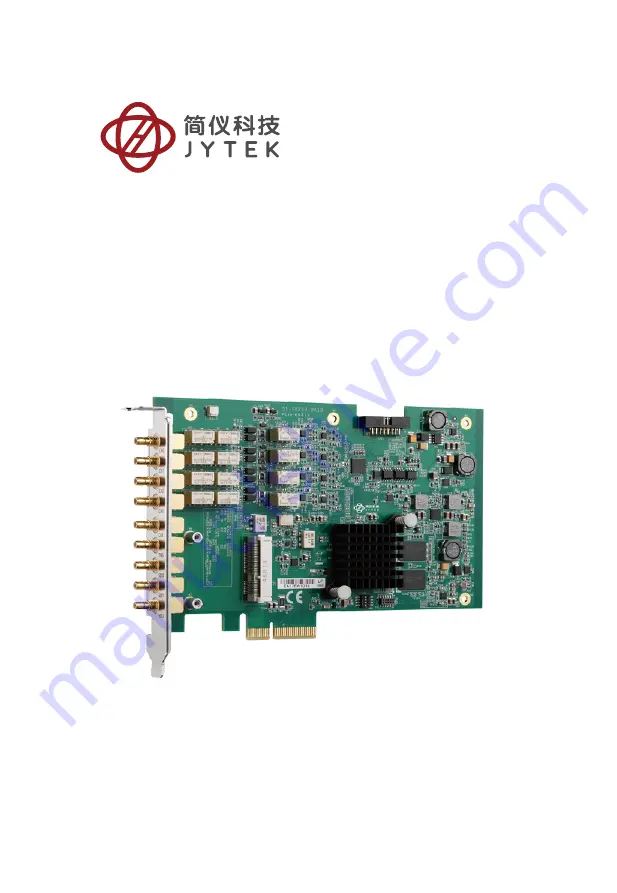
Page 12: ...6 1 5 Device Layout and I O Array All dimensions are in mm Figure 1 2 PCIe 69814 Schematic...
Page 13: ...7 PCIe 69814 I O array is labeled to indicate connectivity as shown Figure 1 3 PCIe 69814 I O Array...
Page 14: ...instrument and initiating acquisition Synced Digital SDI0 3 SDI bits bit 0 2 and ADC data are combined into one register and transferred to host PC by DMA Refer to Chapter 3 for detailed data format...
Page 15: ...e easily damaged by static electricity The module must be handled on a grounded anti static mat The operator must wear an anti static wristband grounded at the same point as the antistatic mat Inspect...
Page 16: ...rew and the bracket cover 4 Line up the PCI express digitizer with the PCI expresss lot on the back panel Slowly push down on the top of the PCI express digitizer until its card edge connector is rest...
Page 17: ...Impe dance Attenuator ADC D river Anti aliasing Filter 0 0 0 0 0 12 12 bit ADC Source Figure 3 1 Analog Input Architecture Input Configuration The input channel terminates with equivalent 50 or 1M in...
Page 18: ...SB Midscale Midscale 1LSB Bipolar Analog Input 4 88mV 0V 4 88mV 2 44mV 0V 2 44mV 0 488mV 0V 0 488mV 0 244mV 0V 0 244mV Digital Code 0001 0000 FFF0 Comment SDI bit is assumed to be 0 Table 3 3 Input Ra...
Page 19: ...aximum DMA data transfer size is 2 MB double words 8 MB bytes in scatter gather mode there is no limitation on DMA data transfer size except the physical storage capacity of the system Users can also...
Page 20: ...Thus the data transfer can reach 80 Mbit s when using internal 80 MS s Timebase clock These three digital input lines are combined with ADC data and located in 3 LSB when SDI function is enabled as s...
Page 21: ...Trigger Architecture The PCIe 69814 requires a trigger to implement acquisition of data Configuration of triggers requires identification of trigger source The PCIe 69814 supports internal software t...
Page 22: ...hat the signal level of the external digital trigger signal should be TTL compatible and the minimum pulse width 20 ns Pulse Width 20ns Pulse Width 20ns Rising Edge Trigger Event Falling Edge Trigger...
Page 23: ...begins Data is generated from ADC and transferred to system memory continuously The acquisition stops once the total data amount reaches a predefined value Figure 3 6 Post Trigger Acquisition Figure 3...
Page 24: ...before the specified amount of data has been acquired are ignored Figure 3 8 Pre Trigger Mode Acquisition 3 4 4 Middle Trigger Mode Collects data before and after the trigger event with the amount to...
Page 25: ...lose to the previous instance will be ignored by the digitizer In Post Trigger mode the minimum spacing between trigger events is N 1 In Delayed Trigger mode the minimum spacing between trigger events...
Page 26: ...source at SMB connector SDI0 generating precisely 80MHz clock for ADC 3 5 3 External Sampling Clock The PCIe 69814 can further choose an external clock source as ADC sampling clock When an external sa...
Page 27: ...ounter is used Using the post trigger mode as an example as shown when a trigger is accepted by the digitizer the acquisition engine commences acquisition of data from ADC and stores the sampled data...
Page 28: ...D ScanIntrv 2 ScanIntrv 3 Figure 3 14 Varying Sampling Rates by Adjusting Scan Interval Counter Counter Name Length Valid Value Description ScanIntrv 16 bit 1 65535 Timebase divider to achieve equival...
Page 29: ...nce clock should be applied The table summarizes SSI functionalities Different signals cannot be routed onto the same trigger bus line SSI Timing Signal Function SSI Trig Input output trigger signal t...
Page 30: ...ch When all sliders are in ON position card number is 15 when all are OFF card number is 0 as shown Slider 1 Slider 2 Slider 3 Slider 4 Card OFF OFF OFF OFF 0 OFF OFF OFF ON 1 OFF OFF ON OFF 2 OFF OFF...
Page 31: ...IG signal to be the trigger event source The signal is configured in the rising edge detection mode 3 8 SDI In some applications marks may need to be added to some data The PCIe 69814 uses SDI to acco...
Page 32: ...ng steps may solve the problem 1 Config SW2 to on 2 Install the module and restart the system 3 If the module is recognized update firmware again ensure the firmware you updated is workable 4 Turn off...
Page 33: ...et to hardware In the absence of user assignment the driver loads constants stored in bank 0 If constants from Bank 1 are to be loaded the preferred bank can be designated as boot bank by software Fol...
Page 34: ...power source settings Always install and operate equipment near an easily accessible electrical socket outlet Secure the power cord do not place any object on over the power cord Only install attach a...