3-10
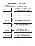
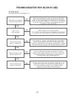
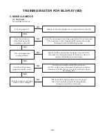
TRAINING MASTER FOR BLU-RAY (BD)
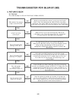
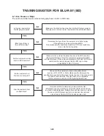
What cables is the customer
using to connect the Bd?
NO
YES
determine what cables the customer is using to connect the Bd
to the tv and if connected properly. refer to oM for connections.
tighten any loose cables. Make sure the customer is not connecting a
Bd to vcr or Bd to dvd recorder. copy protection can distort
the picture on older vcr models.
is the tv set to the
correct input?
NO
YES
Make sure the tv is on the correct input. turn tv off,
then on to determine input. video when using composite,
or component. dvi when using dvi, and hdMi when using hdMi.
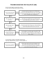
is the customer able to
watch tv programming?
NO
YES
if the customer is not able to watch television then he may have a
problem with his television, especially if the cable signal comes
through on a different input. if the customer can not get a tv program,
then he still may have a problem with the particular input on his tv.
can the customer connect
the Bd to another tv?
NO
YES
have the customer connect the Bd to another tv in order to
determine if the problem is the Bd or the tv. refer to the oM for
connections assistance. if the Bd works on the second tv,
then the customer has a problem with his tv.
has the customer tried
another set of cables?
NO
have the customer try another set of cables. a bad cable
can also cause video problems. test the cable with another device to
the tv to also determine if the tv is bad. if Bd is problem,
please see service chart for service information.
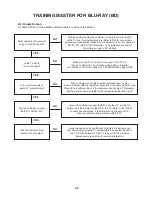
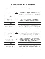
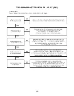
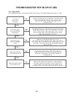
2-4. No Signal
a “no signal” message appears on the screen of the display.
Summary of Contents for XV-BP1B
Page 13: ...2 6 MEMO ...
Page 54: ...3 41 3 Video Part 1 100 Full Color bar 7 9 10 8 11 14 CVBS_I 7 Y 8 Pb 9 Pr 10 ...
Page 56: ...3 43 5 AUDIO PART S PDIF 15 17 16 18 19 21 ASPDIF 15 ...
Page 57: ...3 44 6 HDMI PART 17 16 18 19 21 20 HDMI_SDA 16 HDMI_SCL 17 HDMI_CLK 18 HDMI_DATA 19 ...
Page 58: ...3 45 7 FRONT I F PART 21 20 T_TX 20 R_RX 21 ...
Page 59: ...3 46 BLOCK DIAGRAMS 1 OVERALL BLOCK DIAGRAM ...
Page 60: ...3 47 2 SMPS BLOCK DIAGRAM ...
Page 61: ...3 48 3 SYSTEM BLOCK DIAGRAM ...
Page 62: ...3 49 4 MT8520 DDR2 SDRAM NAND FLASH EEPROM BLOCK DIAGRAM ...
Page 63: ...3 50 5 MT8520 HDMI ETHERNET USB AV BLOCK DIAGRAM ...
Page 65: ...3 52 7 SMPS POWER SIGNAL BLOCK DIAGRAM ...
Page 66: ...3 53 8 MAIN BOARD POWER SIGNAL BLOCK DIAGRAM ...
Page 68: ...3 55 10 LEVEL SHIFTER CEC EFUSE BLOCK DIAGRAM ...
Page 69: ...3 56 MEMO ...
Page 71: ...3 60 3 59 2 POWER TIMER USB CIRCUIT DIAGRAM ...
Page 72: ...3 61 3 62 3 MT8520 1 CIRCUIT DIAGRAM ...
Page 73: ...3 63 3 64 4 MT8520 2 CIRCUIT DIAGRAM ...
Page 74: ...3 65 3 66 5 KEY CIRCUIT DIAGRAM ...
Page 75: ...3 67 3 68 6 TIMER CIRCUIT DIAGRAM ...
Page 76: ...3 69 3 70 7 DDR2 SDRAM CIRCUIT DIAGRAM ...
Page 77: ...3 71 3 72 8 NAND FLASH ETHERNET CIRCUIT DIAGRAM ...
Page 78: ...3 73 3 74 9 AV HDMI CIRCUIT DIAGRAM ...
Page 79: ...3 75 3 76 PRINTED CIRCUIT BOARD DIAGRAMS 1 MAIN P C BOARD TOP VIEW BOTTOM VIEW ...
Page 80: ...3 77 3 78 2 SMPS P C BOARD TOP VIEW BOTTOM VIEW ...
Page 81: ...3 79 3 80 3 KEY P C BOARD TOP VIEW 4 TIMER P C BOARD TOP VIEW BOTTOM VIEW BOTTOM VIEW ...
Page 105: ...4 24 MEMO ...
Page 106: ...4 26 4 25 CIRCUIT DIAGRAM ...
Page 108: ...4 29 4 30 PRINTED CIRCUIT BOARD DIAGRAMS TOP VIEW ...
Page 109: ...4 31 4 32 BOTTOM VIEW ...

