


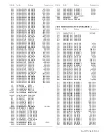


(No.YA711<Rev.002>)1-27
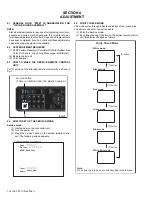
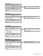
Check SP861,SP862 and their periphery circuit,
and service it if defective.
Are the audio(L/R) signals inputted to Pin(1, 9)
of IC801?
Yes
Yes
Yes
Audio is not outputted normally.(Tuner input)
FLOW CHART NO.3
Are the DIF signals outputted to Pin(26, 28) of CN302?
Check TU302 and their periphery circuit, and service
it if defective.
No
No
Are the audio(L/R) signals outputted to Pin(4, 6)
of IC801?
Check IC801 and their periphery circuit, and
service it if defective.
No
Yes
Are the audio(L/R) signals inputted to Pin(6, 8) of
CN301?
Replace Digital Main PWB Unit.
Check the line between Pin(1, 7) of IC803 and
Pin(1, 9) of IC801, and service it if defective.
Are the audio(L/R) signals inputted to Pin(3, 5)
of IC803?
No
Yes
Check the line between Pin(6, 8) of CN301 and
Pin(3, 5) of IC803, and service it if defective.
Are the audio(L/R) signals outputted to Pin(1, 7)
of IC803?
No
Yes
Replace IC803
No
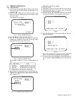
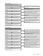
Check SP861,SP862 and their periphery circuit,
and service it if defective.
Are the audio(L/R) signals inputted to Pin(1, 9)
of IC801?
Yes
Yes
Yes
Audio is not outputted normally.(HDMI Audio input)
FLOW CHART NO.4
Are the audio(L/R) signals inputted to Pin(5, 14)
of IC771?
Check the line between Pin(5, 14) of IC771 and input
terminal(JK721, JK722), and service it if defective.
No
No
Are the audio(L/R) signals outputted to Pin(4, 6)
of IC801?
Check IC801 and their periphery circuit, and
service it if defective.
No
Yes
Are the audio(L/R) signals inputted to Pin(6, 8) of
CN301?
Replace Digital Main PWB Unit.
Check the line between Pin(1, 7) of IC803 and
Pin(1, 9) of IC801, and service it if defective.
Are the audio(L/R) signals inputted to Pin(3, 5)
of IC803?
No
Yes
Check the line between Pin(6, 8) of CN301 and
Pin(3, 5) of IC803, and service it if defective.
Are the audio(L/R) signals outputted to Pin(1, 7)
of IC803?
No
Yes
Replace IC803
No
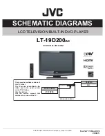
Summary of Contents for LT19D200 - 19" LCD TV
Page 10: ...1 10 No YA711 Rev 002 2 Rear Cabinet S 1 1 Stand Assembly S 2 S 4 S 2 S 2 S 3 Fig D1 ...
Page 70: ...2 54 No YA711 Rev 001 No YA711 Rev 001 2 53 TOP PATTERN DIAGRAMS MAIN PWB PATTERN SOLDER SIDE ...
Page 71: ... No YA711 Rev 001 2 55 2 56 No YA711 Rev 001 R699 TOP MAIN PWB PATTERN PARTS SIDE ...


