background image

2-6

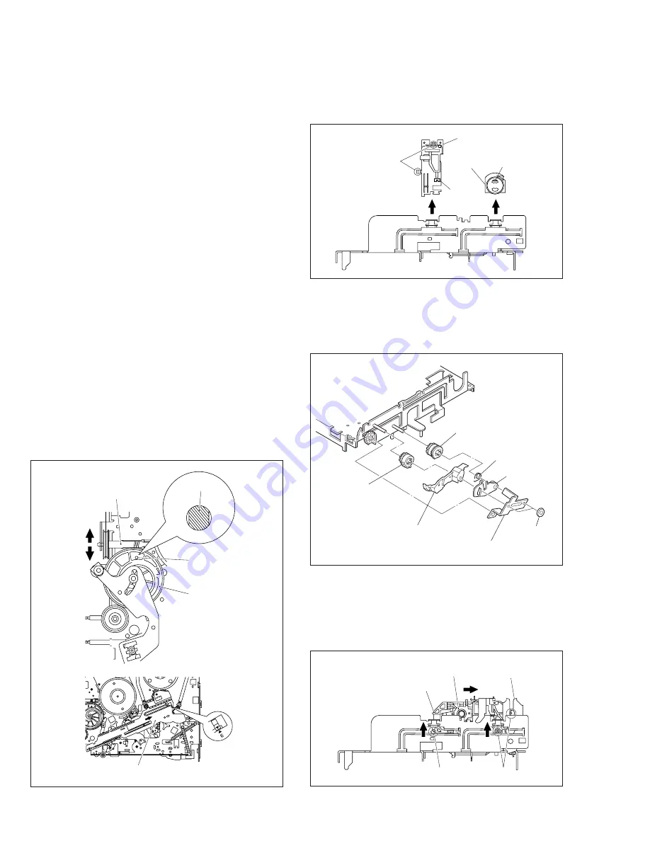
(4) While swinging the lock levers (R) and (L) of the cassette

holder assembly toward the front, slide the cassette
holder assembly until its legs come to where the guide
rail and the roller cam assembly have been removed (so
that the drive arm is upright). (See Fig.2-2-3c.)

Fig. 2-2-3c

Cassette holder assembly

Lock lever (L)

Drive arm

(Upright)

Leg

Legs

2.2.3

Cassette holder assembly

1.  How to remove
(1) Remove the guide rail and roller cam assembly. (See

Fig.2-2-3a.)
(3 lugs on the guide rail and one lug on the roller cam
assembly)

Fig. 2-2-2a

Worm gear

Guide hole

Control cam

Chassis hole

Control plate

Mark E

Fig. 2-2-3b

(2) Remove the two slit washers and remove the cassette

housing bracket. (See Fig.2-2-3b.)

(3) Remove the opener guide, spring(A), door opener, relay

gear and limit gear. (See Fig.2-2-3b.)

Fig. 2-2-3a

Lugs

Lug

Lug

Guide rail

Roller cam 
assembly

Limit gear

Relay gear

Opener guide

Spring(A)

Cassette housing bracket

Slit washers

Door opener

2.2 Replacement of major parts

2.2.1

Before starting disassembling (Phase matching
between mechanical parts)

The mechanism of this unit is closely linked with the rotary
encoder and system controller circuits.
Since the system controller detects the status of mechani-
cal operation in response to phases of the rotary encoder
(internal switch positions), the mechanism may not operate
properly unless such parts as the rotary encoder, control
plate, loading arm gear, control cam, cassette gear, limit gear,
relay gear and drive gear are installed in their correct posi-
tions.
Especially, this model is not provided with any cassette hous-
ing assembly, so that cassette loading and unloading must
be accomplished by operation of the cassette holder assem-
bly. The latter is in turn driven by such parts as the drive
gear, relay gear and limit gear. Exercise enough care, there-
fore, to have the phases of all this gear matching one an-
other. (For information on phase matching of the mechanism,
see the instructions on how to install individual parts.)
This unit is provided with a mechanism assembly mode. It is
therefore necessary to enter this mode for assembling and
disassembling procedures.
This mode is usually not in use, manually set it when it is
required.

2.2.2

How to set the “Mechanism assembling mode”

Remove the mechanism assembly and place it bottom side
up. (See SECTION 1 DISASSEMBLY.) Turn the worm gear
toward the front so that the guide hole of the control cam is
brought into alignment with the hole at the mechanism as-
sembly chassis. This position renders the mechanism assem-
bling mode operational. Make sure that the control plate is
located in alignment with the mark E. (See Fig.2-2-2a.)

Summary of Contents for HR-S9850EK

Page 1: ...m DA4 Double Azimuth head helical scan system Signal to noise ratio 45 dB Horizontal resolution SP LP 250 lines VHS 400 lines S VHS EP 220 lines VHS 350 lines S VHS Frequency range 70 Hz to 10 000 Hz Normal audio 20 Hz to 20 000 Hz Hi Fi audio Input Output 21 pin SCART connectors IN OUT x 1 IN DECODER x 1 RCA connectors VIDEO IN x 1 AUDIO IN x 1 AUDIO OUT x 1 S Video connectors IN x 1 OUT x 1 TUNE...

Page 2: ......

Page 3: ...JUSTMENT 3 1 Precaution 3 1 3 1 1 Required test equipments 3 1 3 1 2 Required adjustment tools 3 1 3 1 3 Color colour bar signal Color colour bar pattern 3 1 3 1 4 Switch settings and standard precautions 3 1 3 1 5 EVR Adjustment 3 1 3 2 Servo circuit 3 2 3 2 1 Switching point 3 2 3 2 2 Slow tracking preset 3 2 3 3 Video circuit 3 2 3 3 1 D A level 3 2 3 3 2 EE Y PB Y S VHS VHS level 3 2 3 3 3 REC...

Page 4: ...e specified for compliance with recognized codes pertaining to X ray emission Consequently when servicing these products replace the cath ode ray tubes and other parts with only the specified parts Under no circumstances attempt to modify these circuits Unauthorized modification can increase the high voltage value and cause X ray emission from the cathode ray tube 12 Crimp type wire connector In s...

Page 5: ...eter to measure across both terminals of load Z See figure 9 and following table 2 5 Grounding Class 1 model only Confirm specified or lower grounding impedance between earth pin in AC inlet and externally exposed accessible parts Video in Video out Audio in Audio out or Fixing screw etc Measuring Method Connect milli ohm meter between earth pin in AC inlet and exposed accessible parts See figure ...

Page 6: ......

Page 7: ...part to be removed unhooked unlocked released unplugged unclamped or unsoldered P Spring W Washer S Screw L Locking tab SD Solder CN WR Remove the wire WR from the connector CN Note 2a When reattaching the Front panel assembly make sure that the door opener a of the Cassette holder assembly is low ered in position prior to the reinstallation When reattaching the Front panel assembly pay careful at...

Page 8: ...rocedures for Lowering the Cassette holder assembly S3b 3 Drum assembly CN1 CON1 WR3a Note 2b L3a L3b P3 Roller arm assy Inertia plate L3c WR3b Note 2b Cleaner assy Not used Not used S3a S3c Drum shield S3d Note When installing the Drum assembly secure the screws S3a to S3c in the order of a b c Turn the loading motor pulley in the direction as indicated by Fig 2 As both A and B levers are lodged ...

Page 9: ...te When installing the Mechanism assembly secure the screws S4a to S4b in the order of a b Fig D4 Fig D6 Fig D5 CN7191 WR5b Note 2b CN7001 WR5a Note 2b L5b L5b 5 SW Display board assembly 5 Jack board assembly Note 5b L5a REC Safety board assembly Note 5a S6c S6b S6a S6b 6 Main board assembly Fig D7 7 Bottom cover L7c L7c L7d L7b L7a L7a L7b S7a Foot assy Foot rear Foot rear Earth plate Note 7a Fo...

Page 10: ... loaded set the switch on the REC safety board assembly to off by releasing the switch 4 Now the desired operation recording playback fast for ward rewind etc is possible in this status 5 The switch on the REC safety board assembly does not have to be operated when ejecting a tape But be sure to turn the set to the normal position before ejecting the tape Note In the Service position the cassette ...

Page 11: ... 2 Transmit the code 36 from the Jig RCU 3 Reset the EMG display Example 1 E 01 03 Previous EMG Latest EMG No EMG record Example 2 E 1 7 1 Displaying the EMG information 1 Transmit the code 59 from the Jig RCU The FDP shows the EMG content in the form of E INITIAL MODE DATA CODE CUSTOM CODE 43 A CODE Data transmitting method Depress the 3 button after the data code is set Jig RCU Notes The EMG det...

Page 12: ...housing load increases during ejection the loading motor is stopped because of lack of headroom in its drive torque Housing load increasing factors Temperature environment low tempera ture etc mechanism wear or failure 3 The sensor switch for detecting the end of ejection are not functioning normally 4 The loading motor drive voltage is lower than specified or power is not sup plied to the motor M...

Page 13: ...EV SEARCH x1 speed reverse playback using JOG CD AUDIO DUB PAUSE EF INSERT REC VIDEO AUDIO PAUSE F0 Mechanism being initialized F1 POWER OFF as a result of EMG F2 Cassette being inserted F3 Cassette being ejected F4 Transition from STOP with pinch roller pressure on to STOP with pinch roller pressure off F5 Transition from STOP with pinch roller pressure on to PLAY F6 Transition from STOP with pin...

Page 14: ...assette thick tape TC 10 09 15 C cassette thick tape TC 20P 0A 0B Small reel thick tape T 20 0A 16 C cassette thin tape TC 30 0A 16 C cassette thin tape TC 40 0D 0F Small reel thick tape T 40 11 14 Small reel thick tape T 60 15 18 Small reel thick tape T 80 DF 160 17 1A Small reel thick tape T 90 DF 180 19 1D Small reel thick tape T 100 1D 21 Small reel thick tape T 120 DF 240 1E 1F Small reel thi...

Page 15: ...layed on the FDP To cancel the copy mode press the PAUSE button of the master unit Player Slave Unit S JLIP cable Recorder Master Unit M CONDITION Power OFF No cassette tape CONDITION Power OFF No cassette tape Flash memory initialization FDP 1 S FDP 2 M FDP 3 M FDP 4 M Completed FDP 5 M Error FDP 1 S 5 Press the STOP button of the master unit When copying is started 3 will be displayed on the FDP...

Page 16: ...ng level Factory reset Note When this operation is executed all user s setting con tents will return to the factory setting level therefore care must be exercised 1 Insert a cassette tape 2 Transmit the code 6F from the Jig RCU 3 After a setting is completed the cassette tape is auto matically ejected 1 Turn on the power 2 Transmit the code FC from the Jig RCU Then the Flash memory utilities scree...

Page 17: ...ch is loaded be cause of any electrical failure manually remove it by taking the following steps 1 Unplug the power cord plug from the power outlet 2 Refer to the disassembly procedure and perform the dis assembly of the major parts before removing the drum assembly 3 Unload the pole base assembly by manually turning the loading motor of the mechanism assembly toward the front In doing so hold the...

Page 18: ... 1 3d 4 In the same way as in the electrical failure instructions in 2 1 3 1 5 remove the top guide 5 Raise the cassette tape cover By keeping it in that posi tion draw out the cassette tape case from the cassette holder and take out the tape 6 By hanging the pinch roller arm assembly spring back on the hook take up the slack of the tape into the cas sette Fig 2 1 3d Fig 2 1 3c Pole base assembly ...

Page 19: ...d Press lever assembly Lid guide Guide arm assembly Reel disk take up side Sub brake assembly take up side Main brake assembly take up side Idler arm assembly Idler lever Main brake assembly supply side Reel disk supply side Rec safety lever Tension brake assembly Adjust pin Tension arm assembly Pole base assembly supply side Full erase head Pole base assembly take up side T1 T26 T25 T24 T23 T22 T...

Page 20: ...y as this will cause damage to the video head 2 To clean the parts of the tape transport system other than the upper drum use a piece of closely woven cloth or a cotton swab soaked with alcohol 3 After cleaning make sure that the cleaned parts are com pletely dry before using the video tape 3 Lubrication With no need for periodical lubrication you have only to lu bricate new parts after replacemen...

Page 21: ...ry encoder B 1 2 2 11 Clutch unit B 1 2 2 12 Change lever assembly B 3 2 2 12 Direct gear B 4 2 2 12 Coupling gear B 5 2 2 12 Clutch gear B 6 2 2 13 Link lever B 1 2 2 14 Cassette gear B 2 2 2 14 Control cam B 2 2 2 14 Worm gear B 1 Lid guide T B 5 2 2 15Control bracket1 B 1 2 2 15Control plate B 6 2 2 16Loading arm gear supply side B 7 2 2 16Loadingarmgear take upside B 8 2 2 16Loading arm gear s...

Page 22: ...ration in response to phases of the rotary encoder internal switch positions the mechanism may not operate properly unless such parts as the rotary encoder control plate loading arm gear control cam cassette gear limit gear relay gear and drive gear are installed in their correct posi tions Especially this model is not provided with any cassette hous ing assembly so that cassette loading and unloa...

Page 23: ...y into the groove See Fig 2 2 3g 4 While swinging the lock lever R of the cassette holder assembly toward the front put the legs A and B into the rail See Fig 2 2 3g 5 Drop the three legs on the left side of the cassette holder assembly into the groove at one time See Fig 2 2 3h 6 Slide the whole cassette holder assembly toward the front to bring it to the eject end position 7 Install the limit ge...

Page 24: ...replacing only the A C head remove the three screws B while controlling the compression spring Fig 2 2 6a Fig 2 2 6c Fig 2 2 4a 2 2 5 Guide arm assembly and press lever assembly 1 How to remove 1 Remove the spring and expand the lug of the lid guide in the arrow indicated direction Then remove the guide arm assembly by pulling it up 2 Remove the press lever assembly by pulling it up See Fig 2 2 5a...

Page 25: ...mbly are correctly in stalled as indicated in Fig 2 2 8b 3 Making sure that the connector for the capstan motor is correctly mounted and securely tighten the three screws A Note When the capstan motor has been replaced with a new one perform recording in the EP or LP mode for at least 2 minutes at normal temperatures immediately be fore starting the FF REW or SEARCH operations Ag ing Spacer Spacer...

Page 26: ...the rotary encoder guide in the arrow indicated direction and remove the change lever assembly 2 Remove the slit washer retaining the direct gear and re move the latter Take care so as not to lose the washer and spring See Fig 2 2 12a 2 2 10 Rotary encoder 1 How to remove 1 Remove the screw A and remove the rotary encoder by pulling it up See Fig 2 2 10a Fig 2 2 10a Rotary encoder Front side Screw...

Page 27: ...t of the rotary encoder guide Mark E Fig 2 2 13c Worm gear Control cam Main deck guide hole Control cam guide hole Cassette gear 2 2 14 Cassette gear control cam and worm gear 1 How to remove 1 Remove the control cam by lifting it 2 Open the two lugs of the cassette gear outward and pull the latter off 3 Remove the belt wound around the worm gear and the loading motor 4 Open the lug of the lid gui...

Page 28: ...embly shaft Section D Section D Section A Hole A 3 Install the control plate so that the section A of the load ing arm gear shaft fits into the hole A of the control plate the section B of the control plate guide into the hole B and the control plate comes under the section C of the rotary encoder guide and the section D of the loading arm gear shaft while press fit the pole base assmebly sup ply ...

Page 29: ...e main deck 3 Remove the lugs B and C of the sub brake assembly take up side from the main deck and remove the sub brake assembly take up side Fig 2 2 19a Spring Sub brake assembly take up side Lug B Lug A Lug C Fig 2 2 20a Lug D Lug C Spring Lug E Lug A Lug B Main brake assembly take up side Reel disk take up side Main brake assembly supply side Notch 2 2 20 Main brake assembly take up side reel ...

Page 30: ...2 Remove the reel disk supply side by loosening in the arrow indicated direction the main brake assembly sup ply side 3 Remove the tension spring on the back of the main deck Then release the lug of the tension arm bearing in the arrow indicated direction and draw out the tension arm assembly See Fig 2 2 21a Fig 2 2 21a Lugs Tension brake assembly Lug of the tension arm bearing Reel disk supply si...

Page 31: ...stall a new washer and upper drum assembly on the drum shaft See Fig 2 2 25a 3 Install the cap to the upper drum assembly 4 Position the collar assembly as indicated in Fig 2 2 25c while controlling its up down movement 5 Secure the collar assembly in position with a hexagonal wrench while pressing its top with the fingers 6 After installation gently turn the upper drum assembly with your hand to ...

Page 32: ...ed See Fig 2 3 1a 5 Reduce the V PB FM waveform by the tracking opera tion If a drop in level is found on the left side turn the guide roller of the pole base assembly supply side with the roller driver to make the V PB FM waveform linear If a drop in level is on the right side likewise turn the guide roller of the pole base assembly take up side with the roller driver to make it linear See Fig 2 ...

Page 33: ...scope Measuring point D TP106 PB FM External trigger E TP111 D FF Adjustment part F A C head base Mechanism assembly Specified value G Maximum V PB FM waveform Adjustment tool H A C head positioning tool PTU94010 1 Play back the alignment tape A1 2 Apply the external trigger signal to D FF E to observe the V PB FM waveform at the measuring point D 3 Set the VCR to the manual tracking mode 4 Loosen...

Page 34: ...point D TP106 PB FM External trigger E TP111 D FF Adjustment part F Jig RCU Code 50 Specified value G STOP mode Maximum V PB FM waveform Adjustment tool H Jig RCU PTU94023B 2 3 5 Tension pole position 1 Play back the back tension cassette gauge A 2 Check that the indicated value on the left side gauge is within the specified value G 3 If the indicated value is not within the specified value G perf...

Page 35: ...304 2 320 4 335 IN FF REW OUT PLAY Direct gear Change lever 2 ON HALF REV HALF FF REW OFF Tension arm ON CONTACT OFF Main brake S ON CONTACT OFF Main brake T ON OFF Sub brake S ON OFF Sub brake T ON OFF OFF ON Capstan brake ON OFF Rec safety switch Operation mode ON PLAY ON REV CONTACT OFF C INS Pinch roller SUPPLY CENTER TAKE UP Idler position READY RESET Take up lever ON OFF Guide arm Timer REC ...

Page 36: ...djustment mode the value is varied with the channel buttons The adjusted data is stored when the setting mode changes from PB to STOP when the tape speed is changed etc Take care to identify the current mode of each adjustment item when making an adjustment When changing the address setting in the EVR adjust ment mode use the Jig RCU or the remote controller having numeric keypad with which a nume...

Page 37: ...e Fig 3 3 1a D A level 1 Insert the cassette tape A3 to enter the mode B 2 Observe the Y OUT waveform at the measuring point D 3 Check the Y level value when the External S input Y C separated video signal 4 Switch the input signal to the External input composite video signal and adjust the adjustment part F so that the Y level becomes the same value observed in step 3 Note The specified value G i...

Page 38: ...confirmation and re adjustment of the item 3 4 1 Fig 3 3 3b REC color colour level V rate Specified value G 7 Set the VCR to the EVR mode by transmitting the code F1 from the Jig RCU 8 Set the EVR address to F2 by transmitting the code F3 from the Jig RCU 9 Transmit the code F4 from the Jig RCU to adjust so that the higher level channel becomes the specified value G of the note B level as shown in...

Page 39: ...marker D2 Specified value G 5 MHz V rate Scale 4 4 div Fig 3 3 4a Video EQ Frequency Response 4 If the A PB FM level is not within the specified value G1 perform the adjustment in a following procedure 5 Set the VCR to the EVR mode by transmitting the code F1 from the Jig RCU 6 Set the EVR address to F2 by transmitting the code F3 from the Jig RCU 7 Transmit the code F4 from the Jig RCU to adjust ...

Page 40: ...VICTOR COMPANY OF JAPAN LIMITED VIDEO DIVISION Printed in Japan S40894 ...

Page 41: ...PB Alignment tape colour bar SP mode normal VHS mode 2 Audio circuits REC 1KHz 8 dBs sine wave signal in SP mode normal VHS mode PB REC then playback it 3 Movie Camera circuits Measured using a correctly illuminated gray scale or colour bar test chatrs in the E E mode 4 Indication on schematic diagram Waveform indications on the schematic diagram are as shown below 5 Waveform indications Waveform ...

Page 42: ... 6 Signal path Symbols The arrows indicate the signal path as follows Playback signal path Playback and recording signal path Recording signal path including E E signal path Capstan servo path Drum servo path Example R Y Y Playback R Y signal path Recording Y signal path 7 Indication of the parts for adjustments The parts for the adjustments are surrounded with the circle as shown below 8 Indicati...

Page 43: ... DRUM MOTOR A C HEAD DEMOD BIT GND BIT OUT DET GND CN7191 CN7192 DET IN FRONT VIDEO GND GND GND GND BIT GND BIT IN ADV JOG 3 FRONT Y IN FRONT C IN F AUDIO R 8 CN7004 JSA JSB GND ADV HEAD PHONE GND HP OUT R HP OUT L CN906 F AUDIO L 38 ADV JOG BS REC CTL CN1 06 CN902 TERMINAL CNR 89 AFC IN GR 96 AFC GND DET OUT M N DET GND AFC IN AFC GND DET OUT M N 7 BS HEAD PHONE 76 REC SAFETY 4 CN301 CN302 74 8 N...

Page 44: ...k 27µ 820p 0 1 12k 1k 680 3 9k 2 2k 0 1 6p 0 01 0 1 68µ 47 1 2k 330p 0 01 0 022 150p 22p 18p 680p 22p 2 2 220 1k 47k 47k 4 7k 680 68k 15µ 0 01 82p 390 1k 6 8k 150p 1 5k 0 001 3 9k 56k 4 7 820 39p 100µ 0Ω 3p 10k 0 033 0 022 12k 150µ 180p 10k 0 01 6 8k 220k 0 012 180 22 4 7 0 0015 0 001 39k 4 7 18k 4 7k 4 7k 100 0 01 10 10 4 7 10k 47 47 0 01 0 01 10µ 2 2k 0 1 10 4 7 0 47 0 47 4 7 10 39k 39k 39k 0Ω 3...

Page 45: ...1 C3041 R3245 R3247 R3246 BS_PCTL H FORCE L R3252 C3007 C3008 C3042 C4017 SEP_PB H AL5V C3043 560 47 0 1M 0 001 0 5 6k 0 22 0 001 0 1 0 1 0 0 0 0 6 8k 22 5 6k 0 0 0 1k 470 4 7k 0 0 0 10k 30p 0 1 100p 4 7k 0 47 10k 1k 1k 1k 10k 560 4 7k 1k 100 1k 1k 1k 470 2 2k 4 7k 1k 1k 0 0 0 0 1k 0 0 0 0 0 0 1 1k 4 7k 0 01 4 7k 100p 0 1k 1k 1k 0 1 5k 0 0 100p 0 330 330 470 470 470 0 0 0 0 1 10k 2 2k 4 7k 10k 0 0...

Page 46: ...5322 D5201 D5211 C5205 C5203 C5202 C5201 C5305 C5204 D5301 R5305 D5303 C5208 L5202 L5201 C5004 R5302 R5334 B5001 LF5001 B5002 F5001 CN5001 Q5304 D5209 C5206 Q5301 R5308 R5309 Q5306 R5310 R5311 Q5302 C5309 B5301 C5308 D5307 Q5305 R5321 R5322 DRUM_12V M12 17 22V V_UP H CP5302 D5305 D5310 AL17V B5305 C5003 CH 12V D5204 B5302 R5319 Q5303 48V R5303 C5307 C5306 RF5V D5214 C5212 Q5320 R5335 R5336 VA5003 ...

Page 47: ...554 JUST_CLK R6021 R6080 R6052 R6051 C6053 C6052 C6022 B6554 C6020 R6551 D6551 C6552 B6510 C6006 C6554 GND Q6501 Q6502 Q6030 Q6031 R6034 R6030 C6033 B6030 AL5V R6032 C6519 C6551 SW_1 C6555 C6021 B6034 B6035 L6501 L6005 R6033 C6520 TU_AUDIO RF_AUDIO R6509 GND TU_VIDEO RF_VIDEO C6023 C6032 R6023 DEMOD R L6050 DEMOD L R6511 SW_2 C6005 D6002 C6016 R6508 SW_1 R6053 C6054 R6510 C6013 C6012 C6008 C6007 L...

Page 48: ...907 EDS H SECAM H CN903 SW_1 B7252 WIDE_DET P MUTE L SW5V 2 MAIN_ALC_DET V PULSE KILLER_DET V P_CTL TRICK H M_TRICK L D FF I2C_DATA_A V I2C_CLK_A V 75 75 75 470 10 220 4 7k 100µ PS_SECAM H BS_ANT FORCE L ANT_CTL H SW12V BIT_IN H SW12V I2C_CLK S P H I2C_DATA GND GND SW12V GND AL6V EE L BS_P CTL H AL17V AL6V SW12V GR_ON H NC NC I2C_CLK I2C_DATA GND TU_VIDEO GND GR_VIDEO F Y_IN GND F C_IN GND BS_AUDI...

Page 49: ...1 R1417 Q1414 R1441 C1462 C1465 C1470 Q1401 R1402 R1401 C1401 C1402 D1401 C1439 L1407 C1446 R1446 C1450 C1452 C1449 C1447 L1405 C1429 R1438 R1440 C1451 D1402 B1409 C1466 C1467 C1469 C1468 Q1406 R1405 Q1404 IC1401 R1454 1 470 10 1 8k 100k 470 6 8µ 0 1 39p 0 01 33k 39k 10µ 330 33p 68p 220 2 2k 2 7k 1µ 1 5k 820 0 1 0 01 100 6 8k 0Ω 680 47 0 1 0 1 0 1 0 1 6 8µ 68p 0 1 33p 560 0 1 4 7 680 27k 0 1 0 1 0...

Page 50: ...0 01 47 0 01 47 15µ 10µH 10µH 10µH 100 100 100 100 4 7µ 4 7µ 4 7µ 0Ω 0 022 15µ 0 1 4 7µ 47 5 6k 3 3k 330p 330p 470p 0 01 5 6k 1µ 470p 470 330p 330p 33p 470p 470p 4 7µ 4 7µ 4 7µ 4 7µ 10 100 470p 47 47 47 0Ω 390 0Ω 100 0 001 10 0 022 0 022 0 022 75 75 330p 330p 1µ 390 100 470p 330p 330p 100 0 22µ 0Ω 470p 1k 75 100 100 10k 0 01 4 7k 0 1k 560 6 8k 2 7k 3 3k 470p 470 0 001 330 0 01 68 1 1 5kΩ 0 47 330 ...

Page 51: ... 47 47 47 47 47 47 47 47 FE 600 FE 600 FE 600 FE 600 FE 600 FE 600 FE 600 FE 600 8p 8p 8p 7p 7p 7p 7p 7p 1p 1p 1p 3p 3p 3p 3p 3p C6708 C6709 X TAL DAC OUT R6713 R6715 C6714 C6716 0 0068 0 0068 0 0068 0 0068 0 0022 0 0022 0 0022 0 0022 VREF C6722 C6723 0 01 0 01 0 01 0 01 0 01 0 01 0 01 0 001 Not used Used IC6701 C6719 C6706 K6701 K6702 C6707 X6701 C6709 C6708 K6703 K6704 R6709 R6708 C6710 C6711 K6...

Page 52: ... C_TO_DIGI Y V_TO_DIGI Y_FROM_DIGI C_FROM_DIGI PB_COLOR V PULSE SECAM_PB_COLOR MAIM_ALC_DET Y_TO_SUB P MUTE L WIDE_DET FRONT_Y_IN FRONT_C_IN FRONT_V_IN REAR2_V_IN V_TO_OSD CHARA_DATA Y_TO_AV V_FROM_AV REC_COLOR REAR1_Y_IN REAR1_C_IN REAR2_Y_IN REAR2_C_IN Y_OUT C_OUT V_FROM_OSD BIAS_FOR_C_OUT GND GND GND GND GND GND 50 25 OPEN OPEN OPEN SHORT 2 CH VC2076DP OPEN OPEN OPEN 16 6 3 50 25 50 50 SW5V SW5...

Page 53: ...4 AN5 PA5 AN6 PA6 AN7 PA7 VREF VDD OSC2 OSC1 VSS XI XO MMOD SD_TOSYS SD_FRSYS SCLK_IN CS_IN RXD_IRPT LN26 O E SLICE IRQ5 P25 P26 RESET TM0IO P10 TM1IO P11 TM2IO P12 TM3IO P13 TM7IO P14 SUB_BUZY TM4IO P16 P17 TXD RXD SBT1 SD_OUT MEM_SIN SCLK_OUT MEM_CS JLIP L DEVICE_SEL OSD_CS OSD_SEL DAVSS DAVDD IOC SLICE_CE AN1 PA1 S CASS H MN101C49GCH OPEN 1Y 0Y 1Z Z COMM 0Z INH VEE GND 0X 1X X COMM Y COMM VCC 7...

Page 54: ... AN0 CS Sin Sout SCLK VEE VEE LED1 LED2 LED3 LED4 G6 M35500BFP M35500BGP M35500AGP 50 OPEN TEST JSA JSB GND ADV RB721Q 40 POWER 29V DC DC GND BUGND RC STB S_DATA_FRSYS S_CLK AL5V S_DATA_TOSYS ADV JOG RCU5V OPE_SW RD9 1ES B2 MTZJ9 1B UZ9 1BSB E PROG INSERT PLAY A DUB SLR 342VC3F REC QSW0905 001 11ES2 1SS133 F F NP NC 6G 5G 4G 3G 2G 1G P16 P15 P14 P13 P12 NC NC NC NC NC P11 P10 P9 P8 P7 P6 P5 P4 P3 ...

Page 55: ...05 R308 R307 R306 B301 Q311 Q312 R301 R321 C301 Q302 C312 C318 C320 C316 L303 R311 C314 R310 R313 C317 R312 R315 R309 R304 R316 C308 C321 IC301 0 47 1 0 0 47 1 1 1 24k 120k 0 0068 0 0068 0 1 0 01 0 01 0 01 6 8µ 27k 150p 47k 2 2k 2 2k 27k 27k 150p 0 001 0 022 0 01 0 01 27µ 3 3k 470p 22k 22k 680p 2 7k 560k 820 6 8k 220k 0 01 300p PB_COLOR V_TO_SECAM SW5V C SYNC GND fsc SECAM H EE L REC_COLOR PB_FM S...

Page 56: ...22 0 22 0 0047 0 22 0 1 0 01 0 01 2 2k 0 0022 5 6k 12k 100k 4 7 120k 5 6k 3 3k 20k 1 10k 100µ 47 1 510 680 390 22k 0 022 4 7 18k 0Ω 0Ω 100 680 330 470 100 1 2k 100 1k 3 3 100 0 01 1 1 0 022 0 01 0 01 0 001 0 0068 0 22 0 01 0 22 0 22 0 22 0 01 0 01 12p 0 01 47 47 47 4 7 47 1 0 47 47 2 2k 1k 1 5k 100µ 390 10k 150k 2 2k 1 2k 22k 1 8k 1k 100 4 7k 100µ 100µ 100k 0 01 0 01 0 01 0 022 100µ 4 7k 0 01 0 01...

Page 57: ...601 A D 5C C3602 B C 5C C3603 B C 6C C3604 B C 6C C3605 B C 6E C3606 B C 6E C3607 B C 6E C3608 B C 5E C3609 B C 5E C3610 A D 6D C3611 A D 6E C3612 B C 10B C3613 B C 10B C3614 B C 6B C3615 B C 1E C3616 B C 11C C3617 B C 11D C3618 B C 11C C3619 B C 11C C3620 B C 6B C3625 A D 12D C3626 A D 10C C3627 A D 10C C3628 A D 9C C3629 A D 9D C3630 B C 15B C3632 B C 10D C3633 B C 3D C3634 A D 3D C3635 A D 4D C...

Page 58: ...4 B C 12N Q35 B C 13M Q37 B C 13N Q38 B C 15M Q39 B C 11O Q41 B C 11O Q401 B C 16J Q402 B C 16J Q403 B C 16I Q404 B C 18G Q405 B C 19G Q2001 B C 14L Q2002 B C 14K Q2003 B C 14L Q2004 B C 14K Q2005 B C 14J Q2006 B C 14K Q2011 B C 14K Q2051 B C 6K Q2052 B C 18H Q2053 B C 18H Q2054 B C 19H Q2061 B C 21G Q2062 B C 19H Q2251 B C 10I Q2252 B C 10I Q3001 B C 7J Q3002 A D 5E Q3003 A D 20E Q3004 B C 3C Q30...

Page 59: ... WR13 WR14 1 120 1 5 1 1 2 12 13 1 19 44 18 43 49 25 8 32 1 2 1 4 3 5 8 9 E 1 4 1 4 3 2 2 33 7 1 85 26 1 11 10 1 8 9 BRN BLU B 1 START SENSOR END SENSOR TAKE UP SUPPLY NEUTRAL 28 29 3 84 4 3 1 2 17 31 30 60 61 1 1 12 1 12 5 4 5 4 8 1 WR12 1 2 10 11 10 6 1 5 8 1 4 3 4 6 1 10 4 5 20 1 8 1 16 V2 1 3 IC3005 IC1 CN1 CN3002 CN501 TU6001 W59 CN902 CN901 C6554 C120 B56 R60 R3256 CN502 CN301 PC3001 D5315 R...

Page 60: ...A C1521 A D 2C CONNECTOR CN1501 A D 3A IC IC1501 B C 2C TRANSISTOR Q1501 A D 3B Q1502 A D 3B RESISTOR R1501 A D 4C R1502 A D 2C R1503 A D 2C R1504 A D 2B R1505 A D 2B R1506 A D 2B R1507 A D 2B R1508 A D 3B R1509 A D 3B R1510 A D 4B R1511 A D 3A R1514 A D 2B R1515 A D 2C R1517 A D 2C 15 S SUB LPB10103 001A 5C C B R535 1D D A C521 RESISTOR TRANSISTOR COIL 2A C B C533 D C C D C C C C D A C551 C554 C5...

Page 61: ... C 5C C1429 A D 3B C1430 A C 2D C1431 A C 2D C1432 B C 2C C1433 A C 3C C1434 B C 3B C1435 B C 1E C1436 B C 2E C1437 A C 3C C1438 B C 3C C1439 A C 5A C1440 B C 3C C1441 A C 3C C1442 B C 4C C1443 B C 4C C1444 A C 4C C1445 A C 4C C1446 A D 5C C1447 B C 5B C1448 A D 5C C1449 A C 4D C1450 A C 3D C1451 A D 5D C1452 A C 3D C1453 A C 3D C1454 A C 2D C1455 B C 2D C1456 A D 5D C1457 A C 5E C1458 A C 5D C145...

Page 62: ...B C920 B C 3B C921 B C 4C C922 B C 4C C923 A D 5B C924 B C 4B C925 B C 3B C926 B C 3B C927 A D 7C C928 B C 9E C929 B C 9E C930 B C 9E C931 A D 8E C932 B C 14D C933 B C 9C C934 B C 9C C935 B C 10E C936 B C 9D C937 B C 8B C938 B C 9B C939 B C 9C C940 B C 9C C941 A D 11E C942 A D 11D C943 A D 4B C944 A D 3B C945 A D 5D C946 A D 5C C947 A D 5D C948 A D 9E C951 A D 5C C952 B C 11A C953 B C 12A C954 A D...

Page 63: ...B C 4A R3321 B C 4C R3322 B C 3A R3323 B C 3A R3326 B C 3B R3328 B C 3B R3329 B C 3B R3330 B C 3B R3331 B C 4B R3332 B C 4C R3333 B C 3C R3339 B C 3C R3340 B C 4C R3342 B C 4D R3343 B C 4C R3345 B C 3C R3346 B C 3C R3347 B C 3C R3348 B C 3C R3349 B C 4C R3350 B C 3C R3351 B C 4D R3352 B C 3D R3363 B C 4D R3364 B C 4C R3371 B C 5C R3372 B C 5C R3373 B C 5C R3374 B C 4D R3386 B C 5B R3401 B C 2E R34...

Page 64: ...STEM CLOCK 10MHz 68 VSS GND 69 OSC2 OUT 70 VCC SYSTEM POWER SYSTEM POWER 71 MODE NC 72 TU_A_MUTE H OUT TUNER AUDIO MUTE CONTROL MUTE H AUDIO MUTE CONTROL MUTE H TUNER VIDEO CONTROL MUTE H 73 TU_V_MUTE H OUT 74 A MUTE H OUT 75 I2C_CLK2 OUT SERIAL DATA TRANSFER CLOCK FOR MEMORY IC SERIAL DATA TRANSFER OUTPUT FOR MEMORY IC 76 I2C_DATA2 IN OUT 77 NC NC 78 NC NC 79 REC_SAFETY IN REC SAFETY SWITCH DETEC...

Page 65: ...20 µsec DIV WF11 4 CN512 4 SECAM PB 0 84 Vp p 20 mV 20 µsec DIV WF1 CN3502 1 FROM_PS_Y REC PB 0 25 Vp p 10 mV 20 WF2 CN3502 3 TO_PS_Y REC PB 1 0 Vp p 50 mV 20 WF3 1 CN3502 5 FROM_PS_C PAL REC PB 0 46 Vp p 10 mV 20 WF3 2 CN3502 5 FROM_PS_C SECAM REC PB 0 64 Vp p 20 mV 20 WF4 1 CN3502 7 TO_PS_C PAL REC PB 0 65 Vp p 20 mV 20 WF4 2 CN3502 7 TO_PS_C SECAM REC 0 52 Vp p 20 mV 20 P S CONVERTER HR S9850MS...

Page 66: ... 11 0 4 6 12 4 0 4 0 13 0 0 14 0 7 0 15 2 4 2 4 16 0 0 17 2 4 2 4 IC201 1 0 0 2 2 5 2 5 3 4 9 4 9 4 0 0 5 4 4 4 4 6 2 4 2 4 7 2 4 2 4 8 4 9 4 9 9 3 3 3 3 10 4 2 4 2 11 1 6 1 6 12 4 9 4 9 13 2 7 2 7 14 2 7 2 7 15 0 0 16 1 2 1 2 17 0 0 18 4 9 4 9 19 2 3 2 3 20 0 0 21 2 3 2 3 22 0 5 0 5 23 4 9 4 9 24 2 9 2 9 25 2 5 2 5 26 4 9 4 9 27 4 6 4 6 28 3 5 3 5 29 4 9 4 9 30 4 9 4 9 IC901 CN911 1 0 0 2 3 0 3 1...

Page 67: ...IC3651 SW2 TU_V_MUTE H I2C_ I2C_ TU_A_MUTE H DATA2 CLK2 SW_1 SW_2 TUNER TO VIDEO AUDIO N REC_ST H FULL_E_ON L N REC_ L H REC_ST H I2C_CLK_A V I2C_DATA_A V A FF A MUTE H TO Vcc X3001 32KHz TIMER X3002 CLOCK MAIN 10MHz TP3905 SP_FG LMC3 LSB LSC LSA 25 27 26 LMC2 LMC1 36 37 35 TU_FG 55 START_SENSOR END_SENSOR 14 66 15 JOGB S_CASS H OSD_CS 91 96 DFG 54 DPG DRUMPWM 107 108 102 CAP_REV L 101 CFG CAPPWM ...

Page 68: ...PB_COLOR 20 25 26 24 23 22 19 17 18 I2C_DATA_A V I2C_CLK_A V Fsc C_TO_DIGI Y V_TO_DIGI 14 15 13 12 USED NOT USED NOT USED NOT Y C Y C C Y C Y Y C C Y C Y Y Y C Y C Y C Y Y Y Y C Y C Y Y Y Y C C C C Y C Note For the waveforms in this block diagram refer to page 4 43 WF11 WF12 WF14 WF13 WF8 WF7 WF9 WF10 WF1 WF2 WF3 WF4 WF5 WF6 FROM_PS_C TO_PS_C TO_PS_Y FROM_PS_Y 9 7 5 3 WF4 WF3 WF2 WF1 C C C C C C Y...

Page 69: ...mph N L R P R P Conv1 Main Det DO DLIM EQ G TRAP P R fH CTL R P CLPF Gen Pulse Delay APC SW ACC Color ID Det L SECAM FM L SECAM COMP SQPB SQPB DL SQPB SEP P EQ LPF ACC HPF R P MUTE TRAP 629 DET AGC R P 2M LPF REC 1 2 Phase Gen 4Phase DOWN SW Conv APC REC APC PB AFC REC 1 2 2FL VCO Discri PB REC SP1 7 VIDEO SIGNAL 8 IC1 CH1 LP1 CH2 CH1 LP2 SP1 LP2 LP1 110 109 108 106 PROCESSOR AUDIO VHS H HARD_SEL ...

Page 70: ... 4 5 CN2001 CN1 HEAD 2 TRANS ERASE FULL 2 1 4 5 HEAD T2051 A ERASE REC PB F ERASE CN2051 A MUTE AMP R CH EVR L CH L CH REDUCTION NOISE NA PB R CH EVR REDUCTION NOISE R CH HIFI CH1 FM CH2 COMMON MON PRE REC NOR DET PROCESSOR SIGNAL AUDIO REC PB DATA ENV LOGIC DET CLK POWER Q2251 97 96 Q2062 A FM TP2253 98 87 SW POWER SW POWER SW SW Q2052 Q2054 59 94 60 93 92 A FF 9 AUDIO ERASE 12 11 10 2 1 6 6 4 11...

Page 71: ... S9850EU LPT0488 005A INST BOOK SP S9850EU LPT0488 006A INST BOOK IT S9850EU REF No PART No PART NAME DESCRIPTION REF No PART No PART NAME DESCRIPTION LPT0488 007A INST BOOK DA S9850EU LPT0488 008A INST BOOK FI S9850EU LPT0488 009A INST BOOK SW S9850EU LPT0488 010A INST BOOK NO S9850EU LPT0488 011A INST BOOK PT S9850EU LPT0488 012A INST BOOK GR S9850EU LPT0488 013A INST BOOK CZ S9850EU LPT0488 014...

Page 72: ...GITAL 2M BOARD ASSY 05 L NAVIGATION BOARD ASSY 19 525 P 516 515 516 B WR2 MECHANISM ASSY M4 P 521 520 520A REC SAFETY BOARD ASSY 32 501J 501F 501E 501 501G 531 532 533 501A 501K 501L 501B ADV JOG BOARD ASSY 38 534 WR6 G A 508 509 507 507 506 WR1 510 510 505 505F 505E 501D 535 SPEC OF BARCODE AUDIO ERASE BOARD ASSY 46 5 2 FINAL ASSEMBLY M2 BEWARE OF BOGUS PARTS Parts that do not meet specifications...

Page 73: ... COVER 513 LP30312 001B BRACKET CHASSIS 514 QYTDSF3010Z SCREW X2 BRACKET CHASSIS 515 LP40700 001A SPECIAL SCREW MECHA 516 QYTDSF3010Z SCREW X2 MECHA 517 QMP4A10 170 POWER CORD S9850EU QMP51K0 170 K POWER CORD S9850EK 519 LP40407 001A KNOB ASSY 520 LP40370 001E ROLLER ARM ASSY 520A PDM4311A 1 ROLLER ASS Y 521 PQ45160 INERTIA PLATE 522 LP40226 001A PC SUPPORT X2 525 PQ40413 SPECIAL SCREW MECHA 526 Q...

Page 74: ...130 137 143 138 139 140 129 127 47 44 43 42 123 AA AA AA AA AA BB AA AA AA AA AA AA AA AA AA AA AA AA BB AA AA AA AA BB 105 120 75 74 121 72 132 76 73 142 88 89 104 135 134 78 107 40 106 49 57 54 59 61 62 85 1 111 60 83 82 52 58 55 39 53 51 1 112 113 151 116 115 117 118 114 119 66 63 68 67 65 64 70 23 25 24 18 19 20 16 27 71 87 22 99 93 96 100 32 94 95 31 80 81 34 37 35 103 32 102 36 38 108 109 90...

Page 75: ...A TENSION ARM ASSY 73 LP30003 010A TENSION SPRING 74 LP40109 003D TENSION BRAKE ASSY 75 PQ46302 1 3 ADJUST PIN 76 LP30232 002A TENSION ARM BEARING 78 LP40532 009B MAIN BRAKE ASSY SUPPLY 80 LP40111 014C MAIN BRAKE ASSY TAKE UP 81 LP30003 029A TENSION SPRING 82 LP40112 001F SUB BRAKE ASSY TAKE UP 83 LP40357 001B TENSION SPRING 84 LP40461 001A CAPSTAN BRAKE ASSY 85 QAR0132 001 CAPSTAN MOTOR 86 QYTDSF...

Page 76: ...RN1309 TRANSISTOR or UN521E TRANSISTOR Q404 DTC144WU TRANSISTOR or PDTC144WU TRANSISTOR or RN1309 TRANSISTOR or UN521E TRANSISTOR Q405 2SA1576A QR X TRANSISTOR Q2001 2SC4081 QRS X TRANSISTOR or 2SD1819A QRS X TRANSISTOR or 2PC4081 R X TRANSISTOR Q2002 2SC4081 QRS X TRANSISTOR or 2PC4081 R X TRANSISTOR or 2SD1819A QRS X TRANSISTOR Q2003 DTA144WU TRANSISTOR or PDTA144WU TRANSISTOR or RN2309 TRANSIST...

Page 77: ... or PDTC114EU TRANSISTOR or RN1302 TRANSISTOR or UN5211 TRANSISTOR Q6032 DTC114EU TRANSISTOR or PDTC114EU TRANSISTOR or UN5211 TRANSISTOR or RN1302 TRANSISTOR Q7201 2SC1317 RS T TRANSISTOR D6 MTZJ5 1C ZENER DIODE D2001 1SS355 DIODE D2202 MTZJ8 2C ZENER DIODE D3001 LNB2301L01VI LE DIODE D3002 1SS133 DIODE D3003 RD39ES B3 T2 ZENER DIODE or MTZJ39C ZENER DIODE D3004 11E2 T5 DIODE D3005 11E2 T5 DIODE ...

Page 78: ...R402 NRSA02J 681X MG RESISTOR 680Ø 1 10W R403 NRSA02J 561X MG RESISTOR 560Ø 1 10W R404 NRSA02J 473X MG RESISTOR 47kØ 1 10W R405 NRSA02J 683X MG RESISTOR 68kØ 1 10W R406 NRSA02J 393X MG RESISTOR 39kØ 1 10W R407 NRSA02J 472X MG RESISTOR 4 7kØ 1 10W R408 NRSA02J 473X MG RESISTOR 47kØ 1 10W R409 NRSA02J 103X MG RESISTOR 10kØ 1 10W R2001 NRSA02J 681X MG RESISTOR 680Ø 1 10W R2002 NRSA02J 272X MG RESISTO...

Page 79: ...R 0Ø 1 10W R3091 NRSA02J 102X MG RESISTOR 1kØ 1 10W R3094 QUY160 100Y IM BUS WIRE R3095 QUY160 100Y IM BUS WIRE R3096 QUY160 100Y IM BUS WIRE R3097 NRSA02J 0R0X MG RESISTOR 0Ø 1 10W R3103 NRSA02J 0R0X MG RESISTOR 0Ø 1 10W R3105 NRSA02J 102X MG RESISTOR 1kØ 1 10W R3106 NRSA02J 102X MG RESISTOR 1kØ 1 10W R3201 NRSA02J 103X MG RESISTOR 10kØ 1 10W R3202 NRSA02J 472X MG RESISTOR 4 7kØ 1 10W R3203 NRSA0...

Page 80: ...00Y IM BUS WIRE R6554 QUY160 100Y IM BUS WIRE R7202 NRSA02J 221X MG RESISTOR 220Ø 1 10W R7203 NRSA02J 472X MG RESISTOR 4 7kØ 1 10W R7204 QRE121J 100Y RESISTOR 10Ø 1 2W R7251 NRSA02J 750X MG RESISTOR 75Ø 1 10W R7252 NRSA02J 750X MG RESISTOR 75Ø 1 10W R7253 NRSA02J 750X MG RESISTOR 75Ø 1 10W B3 NRSA02J 0R0X MG RESISTOR 0Ø 1 10W B18 NRSA02J 0R0X MG RESISTOR 0Ø 1 10W B42 NRSA02J 0R0X MG RESISTOR 0Ø 1 ...

Page 81: ...7 QEKJ1EM 106 E CAPACITOR 10µF 25V C2218 QEKJ1HM 474 E CAPACITOR 0 47µF 50V C2219 QEKJ1EM 106 E CAPACITOR 10µF 25V C2220 QEKJ1HM 475 E CAPACITOR 4 7µF 50V C2221 NCB21HK 103X CAPACITOR 0 01µF 50V C2222 QEKJ1HM 474 E CAPACITOR 0 47µF 50V C2223 QEKJ1HM 474 E CAPACITOR 0 47µF 50V C2224 NCB21HK 103X CAPACITOR 0 01µF 50V C2225 QEKJ1HM 475 E CAPACITOR 4 7µF 50V C2226 QEKJ1EM 106 E CAPACITOR 10µF 25V C222...

Page 82: ...00Z COIL 10µH L6004 QQL29BJ 100Z COIL 10µH L6005 QQL29BJ 100Z COIL 10µH L6032 QUY153 050Y IM BUS WIRE L6501 QUY153 050Y IM BUS WIRE L7201 QQL01BJ 101Z COIL 100µH X1 QAX0576 001 CRYSTAL RESONATOR X2 QCBB1HK 103 CAPACITOR 0 01µF 50V X3001 QAX0445 001 CRYSTAL RESONATOR X3002 QAX0527 001 CRYSTAL RESONATOR S3002 QSW0695 001 PUSH SWITCH S CASS SW K2001 NQL103K R10X COIL 0 1µH K2002 NQL103K R10X COIL 0 1...

Page 83: ...1 10W R1437 NRSA02J 392X MG RESISTOR 3 9kØ 1 10W R1438 NRSA02J 473X MG RESISTOR 47kØ 1 10W R1439 NRSA02J 273X MG RESISTOR 27kØ 1 10W R1440 NRSA02J 473X MG RESISTOR 47kØ 1 10W R1441 NRSA02J 682X MG RESISTOR 6 8kØ 1 10W R1442 NRSA02J 682X MG RESISTOR 6 8kØ 1 10W R1446 NRSA02J 102X MG RESISTOR 1kØ 1 10W R1447 NRSA02J 102X MG RESISTOR 1kØ 1 10W R1448 NRSA02J 102X MG RESISTOR 1kØ 1 10W R1449 NRSA02J 10...

Page 84: ...r 2SC4081 QRS X TRANSISTOR or 2PC4081 R X TRANSISTOR Q908 2SB1218A QR X TRANSISTOR or 2PA1576 R X TRANSISTOR or 2SA1576A QR X TRANSISTOR Q909 2SB1218A QR X TRANSISTOR or 2SA1576A QR X TRANSISTOR or 2PA1576 R X TRANSISTOR Q911 UN521E TRANSISTOR or RN1309 TRANSISTOR or DTC144WU TRANSISTOR or PDTC144WU TRANSISTOR Q912 UN5215 TRANSISTOR or RN1311 TRANSISTOR or DTC114TU TRANSISTOR or PDTC114TU TRANSIST...

Page 85: ...CAPACITOR 0 022µF 50V C921 NDC21HJ 330X CAPACITOR 33pF 50V C923 QEKJ1CM 476 E CAPACITOR 47µF 16V C924 NCB21HK 103X CAPACITOR 0 01µF 50V C925 NCB21HK 223X CAPACITOR 0 022µF 50V C927 QEKJ1CM 476 E CAPACITOR 47µF 16V C930 NCB21HK 103X CAPACITOR 0 01µF 50V C931 QEKJ1CM 476 E CAPACITOR 47µF 16V C933 NCB21HK 331X CAPACITOR 330pF 50V C934 NCB21HK 331X CAPACITOR 330pF 50V C935 NCB21HK 471X CAPACITOR 470pF...

Page 86: ...PA10103 07A S SUB BOARD ASSY IC501 JCP8018 IC or JCP8028 IC or JCP8038 IC or JCP8028 01 IC IC502 VC2076DP IC R503 NRSA02J 221X MG RESISTOR 220Ø 1 10W R504 NRSA02J 332X MG RESISTOR 3 3kØ 1 10W R505 NRSA02J 392X MG RESISTOR 3 9kØ 1 10W R506 NRSA02J 391X MG RESISTOR 390Ø 1 10W R507 NRSA02J 122X MG RESISTOR 1 2kØ 1 10W R508 NRSA02J 151X MG RESISTOR 150Ø 1 10W R509 NRSA02J 162X MG RESISTOR 1 6kØ 1 10W ...

Page 87: ...RSA02J 0R0X MG RESISTOR 0Ø 1 10W R3343 NRSA02J 0R0X MG RESISTOR 0Ø 1 10W R3345 NRSA02J 0R0X MG RESISTOR 0Ø 1 10W R3346 NRSA02J 0R0X MG RESISTOR 0Ø 1 10W R3347 NRSA02J 0R0X MG RESISTOR 0Ø 1 10W R3348 NRSA02J 0R0X MG RESISTOR 0Ø 1 10W R3349 NRSA02J 0R0X MG RESISTOR 0Ø 1 10W R3350 NRSA02J 0R0X MG RESISTOR 0Ø 1 10W R3351 NRSA02J 0R0X MG RESISTOR 0Ø 1 10W R3352 NRSA02J 0R0X MG RESISTOR 0Ø 1 10W R3371 N...

Page 88: ... B7003 QUY160 100Y IM BUS WIRE C7001 QCFB1HZ 104 CAPACITOR 0 1µF 50V C7007 QETN1HM 476 E CAPACITOR 47µF 50V C7009 QCSB1HJ 150 CAPACITOR 15pF 50V C7010 QCFB1HZ 104 CAPACITOR 0 1µF 50V C7011 QETN1AM 227 E CAPACITOR 220µF 10V C7019 QDVB1EZ 223Y CAPACITOR 0 022µF 25V C7023 QEKC1HM 106 E CAPACITOR 10µF 50V L7001 QQL29BK 1R0Z COIL 1 0µH S7001 QSW0456 002Z TACT SWITCH POWER S7002 QSW0456 002Z TACT SWITCH...

Page 89: ...19A QRS X TRANSISTOR R2054 NRSA02J 153X MG RESISTOR 15kØ 1 10W R2055 NRSA02J 3R3X MG RESISTOR 3 3Ø 1 10W C2052 QFLC1HJ 333Z F CAPACITOR 0 033µF 50V C2053 NCB21HK 332X CAPACITOR 0 0033µF 50V C2054 NCB21HK 103X CAPACITOR 0 01µF 50V C2055 QEKJ1CM 106 E CAPACITOR 10µF 16V T2051 PELN0860 OSC TRANSFORMER CN2052 QGB2024J1 04S CONNECTOR 1 4 MAIN LOADING MOTOR BOARD ASSEMBLY 55 PW2 LPA10010 01A2 L MOTOR BO...

Page 90: ......

Reviews: