background image

(No.22062)1-23

3.3

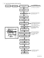
Flow of functional operation until TOC read (CD)

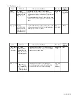
Slider turns REST
      SW ON.

Automatic tuning
of TE offset

Laser ON

Detection of disc

Automatic measurement of
Focus A-curve amplitude

Automatic tuning of
   Foucus offset

Disc is rotated

Focus servo ON
(Tracking servo ON)

Automatic tuning of
Tracking error balance

Automatic measurement of
Tracking error amplitude

Automatic tuning of
Focus error balance

Disc to be
braked to stop

Tracking
servo
on statas

Tracking
servo
off statas

Disc statas
to rotate

TOC reading
  finishes

Automatic measurement

of TE amplitude and 

automatic tuning of

TE balance

500mv/div
 2ms/div

Fig.1

Approx.3sec

pin 20 of
IC601(TE)

Approx
 1.8V

VREF

Tracking error waveform at TOC reading

Power ON

Power Key

Confirm that the Focus error
S-cuve siganl at the pin23 of
IC601 is approx.2Vp-p

Confirm that the siganl from
pin22 IC603 is 0V as a 
accelerated pulse during 
approx.400ms.

Confirm the waveform of
the Tracking error signal
at the pin20 of IC601
(See fig-1)

Automatic tuning of
Focus error gain

Automatic tuning of
Tracking error gain

TOC reading

Play a disc

Confirm the eys-pattern
at the lead of TP1

Check that the voltage at the pin4

of CN601 is 0V (a moment)?

Check Point

Check that the voltage at the 

pin2 of IC601 is 0V?

Summary of Contents for FS-H30

Page 1: ...Y OF JAPAN LIMITED No 22062 2003 5 COMPACT COMPONENT SYSTEM 22062 2003 5 FS H30 TABLE OF CONTENTS 1 Precautions 1 3 2 Disassembly method 1 7 3 Adjustment 1 19 4 Description of major ICs 1 25 COMPACT COMPONENT SYSTEM Area Suffix J U S A C Canada ...

Page 2: ...ning range 530 kHz 1 710 kHz CD player Dynamic range 85 dB Signal to noise ratio 90 dB Wow and flutter Immeasurable Cassette deck Frequency response Normal type I 50 Hz 15 000 Hz Wow and flutter 0 15 WRMS Speaker Speaker units Full range 8 0 cm 3 3 16 in cone 1 Impedance 4 Ω Dimensions approx 135 mm 203 mm 190 mm W H D 5 3 8 in 8 in 7 1 2 in Mass approx 1 7 kg 3 8 lbs each General Power requiremen...

Page 3: ...ack control shafts etc to be sure the product is safe to operate without danger of electrical shock Do not use a line isolation transformer during this check Plug the AC line cord directly into the AC outlet Using a Leakage Current Tester measure the leakage current from each exposed metal parts of the cabinet particular ly any exposed metal part having a return path to the chassis to a known good...

Page 4: ...es type of fast operating fuse Precaution Pour eviter risques de feux remplacez le fusible de surete de F901 comme le meme type que 1A 125V et 6 3A 125V pour F902 et F903 Ce sont des fusibles suretes qui functionnes rapide C902 C901 C903 C904 CN901 D901 D902 D904 D903 D905 Z901 Z913 Z902 T901 J902 L901 R901 S901 Z912 B908 Z903 Z911 PP901 B910 B911 B914 B913 B916 B902 B901 B903 B904 B909 B907 B912 ...

Page 5: ...ptical pickup The tester s internal power source can easily destroy the laser diode 1 7 Handling the traverse unit optical pickup 1 Do not subject the traverse unit optical pickup to strong shocks as it is a sensitive complex unit 2 Cut off the shorted part of the flexible cable using nippers etc after replacing the optical pickup For specific details refer to the replacement procedure in the text...

Page 6: ... equipped with safety switches which prevent emission of radiation when the drawer is open and the safety interlocks have failed or are de feated It is dangerous to defeat the safety switches 5 CAUTION If safety switches malfunction the laser is able to function 6 CAUTION Use of controls adjustments or performance of procedures other than those specified herein may result in hazardous radiation ex...

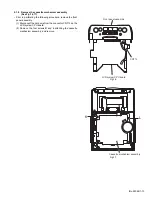
Page 7: ...1 Removing the rear panel See Fig 1 2 1 From behind the body remove the eight screws A attach ing the rear panel 2 Turing the body upside down remove the two screws B at taching the rear panel and remove Fig 1 Fig 2 A A A A B B C C Front panel assembly Rear panel ...

Page 8: ...wo screws C attaching the front panel assembly 2 Turning the body initial position open the CD door while pressing the upper OPEN button 3 Moving the side panel L in the arrow direction remove the panel from the left side of the body 4 Moving the side panel R in the arrow direction remove the panel from the right side of the body Fig 3 Fig 4 Fig 5 Side panel L Side panel R ...

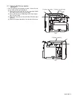
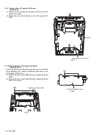
Page 9: ...ard wires from the two connectors CN603 and CN604 on the CD servo control board 2 Remove the two screws D attaching the front panel assem bly on the both sides 3 Release the two joints a on the both sides of the front panel assembly 4 Move the CD player assembly in the direction of the arrow Fig 6 Fig 7 CD player assembly CD servo control board CN604 D a CN603 D CD player assembly a ...

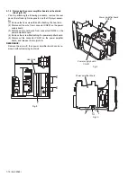
Page 10: ...om connector CN901 on the power supply board 3 Disconnect the card wire from connector CN305 on the power amplifier board 4 Remove the screw G attaching the power amplifier board 5 Disconnect the connector CN301 on the power amplifier board and release the two joints b REFERENCE Remove the screw F then power amplifier board can be re moved without removing heat sink Fig 8 Fig 9 Fig 10 E E F Heat s...

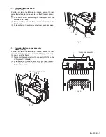
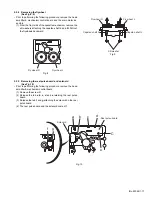
Page 11: ...t c and remove the tuner board backward Fig 11 2 1 6 Removing the front panel assembly See Fig 12 13 Prior to performing the following procedure remove the rear panel the left and right side panels the CD player assembly the power amplifier board 1 Disconnect the card wire from the connector CN714 on the LCD system CPU board 2 Release the joint d on the bottom of the front panel assem bly using a ...

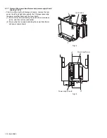
Page 12: ...el the left and right side panels the CD player assembly the power amplifier board and the tuner board 1 Remove the screw I attaching the jack holder and release joint e and then remove jack holder 2 Remove the four screws J attaching the power transformer and power supply board Fig 14 Fig 15 I Jack holder e J J Power transformer Power supply board ...

Page 13: ...ing procedure remove the front panel assembly 1 Disconnect the card wire from the connector CN713 on the LCD system CPU board 2 Remove the four screws K and L attaching the cassette mechanism assembly and remove Fig 16 Fig 17 Front panel assembly LCD system CPU board CN713 K L Cassette mechanism assembly ...

Page 14: ...Removing the operating switch board See Fig 19 20 Prior to performing the following procedure remove the front panel assembly the cassette mechanism assembly and the LCD system CPU board 1 Remove the two screws M attaching the operating switch button 2 Remove the two screws N attaching the operating switch board and remove Fig 19 Fig 20 f LCD system CPU board CN716 M Operating switch button N Oper...

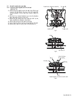
Page 15: ...ise as you turn the flywheel R counterclockwise See Fig 2 and 3 3 Disconnect the flexible wire from connector CN31 on the head amplifier mechanism control board 4 Remove the spring from the back of the head 5 Loosen the azimuth screw for reversing attaching the head 6 Remove the head on the front side of the head mount Fig 1 Fig 2 Fig 3 Cassette mechanism assembly Fly wheelR Trigger arm Head mount...

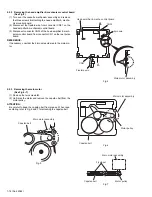
Page 16: ... pulse board REFERENCE If necessary unsolder the 4 pin wire soldered to the main mo tor Fig 4 2 2 3 Removing the main motor See Fig 4 7 1 Remove the two screws B 2 Half raise the motor and remove the capstan belt from the motor pulley ATTENTION Be careful to keep the capstan belt from grease When reas sembling refer to Fig 6 and 7 for attaching the capstan belt Fig 5 Fig 6 Fig 7 Head amplifier mec...

Page 17: ...ard Fig 8 Fig 9 2 2 5 Removing the reel pulse board and solenoid See Fig 10 Prior to performing the following procedure remove the head amplifier mechanism control board 1 Remove the screw C 2 Release the tab a b c d and e retaining the reel pulse board 3 Release the tab f and g attaching the solenoid on the reel pulse board 4 The reel pulse board and the solenoid come off Fig 10 Fly wheel R Fly w...

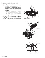
Page 18: ...the left to disengage the gear If the gear can not be disengaged easily push up the boss Q slightly and raise the rear side of the head mounts slightly to return the direction lever to the reversing side 2 Tighten the azimuth screw for reversing 3 Reattach the spring from the back of the Play Record Clear head 4 Connect the flexible wire to connector CN31 on the head amplifier mechanism control bo...

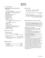
Page 19: ...nal to this terminal This system is of an BTL system 8 For connecting a dummy resistor when measuring the output use the wire with a greater code size 9 Whenever any mixed tape is used use the band pass filter DV 12 Measurement conditions Power supply voltage AC 120V 60Hz Reference output Speaker 0 775V 4 Headphone 0 077V 32 Reference frequency and input level 1kHz AUX 8dBs Measurement output term...

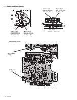
Page 20: ... C103 C105 C106 C107 C209 C110 C113 C121 C101 C202 C203 C205 C206 C207 C109 C210 C213 C221 C300 C301 C304 C306 C307 C308 C310 C313 C314 C316 C319 C331 C340 C341 C342 C371 C374 C376 CN31 CN33 CN34 D340 D375 IC32 IC33 L301 L303 Q302 Q305 Q342 Q343 Q344 Q345 Q346 Q371 Q372 Q375 Q376 R101 R102 R104 R105 R106 R107 R108 R110 R116 R121 R201 R202 R204 R205 R206 R207 R208 R210 R216 R221 R301 R302 R303 R304...

Page 21: ...712 3kHz Output terminal Speaker out or Headphone out Playback the test tape VT712 3kHz at end of forward and reverse tape speed deviation should be less than 6 0Hz Playback the test tape VT712 3kHz at end of forward side adjust to 2 940 3 90Hz indication of frequency counter by VR37 VR37 Tape speed diviation at FWD REV Test tape VT712 3kHz Output terminal Speaker out or Headphone out Leass than 6...

Page 22: ...Lch and VR32 for Rch VR31 VR31 AC 225 4 20 A AC 514 4 0 A Output deviation 1kHz 10kHz 1dB 2dB Item Condition Measurement method Ref value Adjustment position Forward or Reverse Test tape AC 514 TYPE AC 225 TYPE Output terminal Recording head 1 Set the test tape AC 514 TYPE and AC 225 TYPE then make REC PAUSE condition 2 Release the PAUSE to REC condition connect 1W to ERASE head by series then con...

Page 23: ...nishes Automatic measurement of TE amplitude and automatic tuning of TE balance 500mv div 2ms div Fig 1 Approx 3sec pin 20 of IC601 TE Approx 1 8V VREF Tracking error waveform at TOC reading Power ON Power Key Confirm that the Focus error S cuve siganl at the pin23 of IC601 is approx 2Vp p Confirm that the siganl from pin22 IC603 is 0V as a accelerated pulse during approx 400ms Confirm the wavefor...

Page 24: ...l block do not touch the semi fixed resistor If the laser power is lower than the specified value the laser diode is almost worn out and the laser pickup should be replaced If the semi fixed resistor is adjusted while the pickup is functioning normally the laser pickup may be damaged due to excessive cur rent 3 5 Replacement of laser pickup CD Replace it NO YES O K Is the level of RFOUT under 1 25...

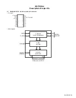
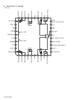
Page 25: ...ort extension Pin layout Block diagram STROBE DATA CLOCK Q1 Q2 Q3 Q4 Vss Vdd OUTPUT ENABLE Q5 Q6 Q7 Q8 Q s Qs 1 2 3 4 5 6 7 8 16 15 14 13 12 11 10 9 8 STAGE SHIFT REGISTER 8 BIT LATHES 3 STATE OUTPUTS 1 2 3 15 Q1 Q8 10 9 DATA CLOCK STROBE OUTPUT ENABLE PARALLEL OUTPUT Q s Qs SERIAL OUTPUT ...

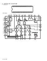
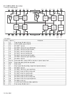
Page 26: ...25 26 27 28 29 30 31 32 AMP GCA BCA AMP GCA BCA AMP GCA BCA AMP GCA BCA RF_EQ AGC BDO OFTR 3TENV NRFDET SUBT SUBT VDET GCTL TBAL FBAL GND VCC PD LD VDET TEBPF TEOUT TEN FEOUT FEN NRFDET 3TOUT CEA OFTR COFTR BDO BCDO ARF CAGC RFIN RFOUT RFN A C B D E F VREF 4 5 6 7 8 11 12 13 14 9 10 15 22 23 21 20 19 18 2 1 3 16 25 26 24 17 28 27 29 30 31 32 ...

Page 27: ...citor connecting terminal for envelope detection on the light side 14 OFTR O OFTR output terminal 15 NRFDET O NRFDET output terminal 16 GND Ground 17 VREF O VREF output terminal 18 VDET O VDET output terminal 19 TEBPF I VDET output terminal 20 TEOUT O TE Amp output terminal 21 TEN I TE Amp inverting input terminal 22 FEN I FE Amp inverting input terminal 23 FEOUT O FE Amp output terminal 24 GCTL O...

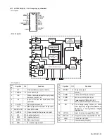
Page 28: ...L TAI L PB OUT L REC IN L ALC L REC OUT L NC NC NC EQ MUTE MUTE Return SW Return SW ALC EQ NC TEST Open for nomal use REC MUTE OFF ON MUTO ON OFF REC RETURN ON OFF TEST 4 ALC ON OFF Vcc PB NF1 L TEST 2 RIP PBIN l REC Return GND PBIN R NC TEST 3 PB NF1 R 1 2 3 4 5 6 7 8 9 10 20 19 18 17 16 15 14 13 12 11 31 32 33 34 35 36 37 38 39 40 30 29 28 27 26 25 24 23 22 21 ...

Page 29: ...Return ON OFF Mode control input 16 Vcc Vcc Pin 17 ALC DET ALC detection signal out put 18 GND GND pin 19 I REF Equalizer reference current input 20 Test mode Test modepin 21 REC OUT L REC output 22 NC NC pin 23 ALC L ALC L signal out put 24 REC IN L REC EQ input 25 NC NC pin 26 PBOUT L PB output 27 TAI L Tape input 28 EQOUT L EQ output 29 PB EQ L NAB output 30 PB NF2 L PB EQ feed back 31 PB NF1 L...

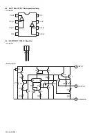
Page 30: ...mp Pin layout 4 6 KIA78S05P T IC604 Regulater Pin layout Block diagram 8 7 6 5 VCC Vout2 Vin 2 Vin 2 Vout1 Vin 1 Vin 1 VEE 1 2 3 4 1 2 3 INPUT 1 OUTPUT Q3 Q5 Q12 Q13 R7 R5 R6 R8 Q11 Q10 Q9 C1 Q6 R2 R3 Q7 Q8 Q2 R11 R10 Q16 R9 Q1 Q14 Z1 R1 Q4 R4 2 COMMON ...

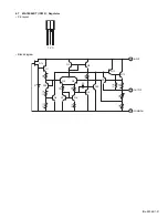
Page 31: ... No 22062 1 31 4 7 KIA78S06P T IC932 Regulator Pin layout Block diagram 1 2 3 Q14 Q12 Q13 Q10 Q11 Q4 Q3 Q5 Q6 Q1 Q2 Q7 Q8 Q9 Z1 R9 R3 R4 R1 R2 R8 R7 R5 R6 Q16 R11 R10 C1 3 INPUT 1 OUTPUT 2 COMMON ...

Page 32: ... 10 AM SD This is a terminal of AM ceramic filter 11 FM VSM O Adjust FM SD sensitivity 12 AM VSM O Adjust AM SD sensitivity 13 MUTE I O When the signal of IF REQ of IC121 LC72131 appear the signal of FM AM IF output Muting control input 14 FM AM I Change over the FM AM input H FM L AM 15 MONO ST O Stereo H Mono L 16 L OUT O Left channel signal output 17 R OUT O Right channel signal output 18 L IN ...

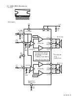
Page 33: ...Output Amp Ripple Filter Starting Time POLYESTER FILM CAPACITOR OUTPUT GND SHORT OUTPUT VCC SHORT RL SHORT PROTECTION CIRCUITS THERMAL SHUTDOWN CH 1 CH 2 IN2 Ri 20k Input Amp Input Amp PRE GND Ri 20k 4 7 10V 5 6 2 3 4 STAND BY SIGNAL MUTE 22K 7 8 14 13 12 9 10 11 VCC1 VCC2 VCC RL 4 to 8 RL 4 to 8 2200 25V 2 2 0 1 0 1 2 2 2 2 0 1 4 7 10V 4 7 25V ...

Page 34: ...2 BTL AMP 1 input pin Inverting side 7 Vo3 BTL AMP 2 input pin Inverting side 8 Vo4 BTL AMP 2 input pin Non inverting side 9 Vg2 BTL AMP 2 input pin For gain adjustment 10 Vin2 BTL AMP 2 input pin 11 Reg Out External transistor collector PNP connection 5V power supply output 12 Reg In External transistor PNP base connection 13 Res Reset output 14 Cd Reset output delay time setting Capacitor connec...

Page 35: ...or 4pin input and 6pin output H 4 DI I Input for receive the serial data from controller 5 CLOCK I Sync signal input use 6 DO O Data output for Controller Output port 7 FM ST VCO O Low MW mode 8 AM FM O Open state after the power on reset 9 LW I O Input output port 10 MW I O Input output port 11 SDIN I O Data input output 12 IFIN I IF counter signal input 13 IFCONT O IF signal output 14 Not use 15...

Page 36: ... Test input 8 XOUT O Crystal oscillator output 4 332MHz 9 XIN I Crystal oscillator input exeternal reference input 10 Vssd Digtal ground 11 Vddd Digtal power supply 12 MODE I Read mode setting 0 master 1 slave 13 RST I RDS ID RAM reset positive polarity 14 RDDA O RDS data output 15 RDCL I O RDS clock output master mode RDS clock input slave mode 16 RDS ID READY O RDS ID READY output negative polar...

Page 37: ...Volume control and equalizer input 10 LSEL0 Input selector output 11 L4 Not used 12 L3 Input signal connections not used 13 L2 Input signal connections 14 L1 Input signal connections 15 NC GND 16 NC GND 17 R1 Input signal connections 18 R2 Input signal connections 19 R3 Input signal connections not used 20 R4 Not used 21 RSEL0 Input selector output 22 RIN Volume control and equalizer input 23 RTRE...

Page 38: ...Off track 37 TRCRS I Track cross signal input 38 RFDET I RF detect signal input L Detect 39 BDO I Drop out signal input H Drop out 40 LDON O Laser on signal output 41 PLLF2 Not use 42 TOFS Not use 43 WVEL Not use 44 ARF I RF signal input 45 IREF I Reference current input 46 DRF I Bias pin for DSL 47 DSLF I O Loop filter pin for DSL 48 PLLF I O Loop filter pin for PLL 49 VCOF I O Loop filter pin fo...

Page 39: ... O CD Function H CD 27 STAT I CD status input port 28 MUTE O BTL mute control port MUTE ON L 29 RST CLOSE O Door close detection 30 VOLCE I Volumn Chip Enable 31 BCTL I Switched 5V control H 5V off 32 BUP I Back up power detect H BACKUP 33 _REM I Remote control input 34 RDSCK I RDS clock 35 BLKCK Block clock input port 36 FLAG Error Correction Count 37 38 Not use 39 VDD O 5V 40 VREF O 5V 41 _XRST ...

Page 40: ... No 22062 AV MULTIMEDIA COMPANY AUDIO VIDEO SYSTEMS CATEGORY 10 1 1chome Ohwatari machi Maebashi city 371 8543 Japan VICTOR COMPANY OF JAPAN LIMITED WPC Printed in Japan ...

Reviews: