background image

1-9

FS-A52

Prior to performing the following procedure, remove 
the rear cover, the side panels, the top panel and the 
system control board.

Release the two joints 

d

  on the lower right and left 

sides of the front panel assembly, then remove the 
front panel assembly toward the front.

1.

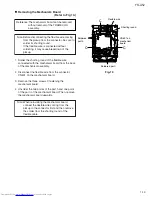
Removing the front panel assembly 

(See Fig.11 and 12)

Prior to performing the following procedure, remove 
the rear cover, the side panels, the top panel, the 
system control board and the front panel assembly 
section.

Disconnect the wire from connector CN804 on the 
main board.

Remove the plastic rivet fixing the headphone jack 
board.

1.

2.

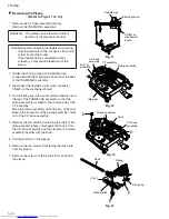
Removing the headphone jack board

(See Fig.13 and 14)

Fig.11

Fig.12

Fig.13 

Fig.14

Front panel assembly

Front panel assembly

Joint d

Joint d

Headphone jack board

Headphone jack board

Main board

CN804

Plastic rivet

Summary of Contents for FS-A52

Page 1: ...y Disassembly method Contents Adjustment method Flow of functional operation until TOC read CD Maintenance of laser pickup Replacement of laser pickup Description of major ICs 1 2 1 3 1 4 1 5 1 6 1 25 1 29 1 30 1 30 1 31 48 STANDBY ON COMPACT DIGITAL AUDIO COMPACT COMPONENT SYSTEM FS A52 PHONES COLOR CLOCK TIMER FM MODE DISPLAY SOUND MODE AHB PRO SET CANCEL CD DIMMER FM AM REV MODE REPEAT TAPE STA...

Page 2: ...uct antenna terminals knobs metal cabinet screw heads headphone jack control shafts etc to be sure the product is safe to operate without danger of electrical shock Do not use a line isolation transformer during this check Plug the AC line cord directly into the AC outlet Using a Leakage Current Tester measure the leakage current from each exposed metal parts of the cabinet particularly any expose...

Page 3: ...a tester to check the condition of the laser diode in the optical pickup The tester s internal power source can easily destroy the laser diode 4 Handling the traverse unit optical pickup 1 Do not subject the traverse unit optical pickup to strong shocks as it is a sensitive complex unit 2 Cut off the shorted part of the flexible cable using nippers etc after replacing the optical pickup For specif...

Page 4: ...es malfunction the laser is able to function 6 CAUTION Use of controls adjustments or performance of procedures other than those specified herein may result in hazardous radiation exposure VARNING Osynlig laserstrålning är denna del är öppnad och spårren är urkopplad Betrakta ej strålen VARO Avattaessa ja suojalukitus ohitettaessa olet alttiina näkymättömälle lasersäteilylle Älä katso säteeseen AD...

Page 5: ...ame type 1 25A 125V for F1001 2 5A 125V for F1003 and 5A 125V for F1004 This symbolspecifies type of fast operating fuse Precaution Pour evitisques de fer reux remplacez le fusible de surete de F1001 comme le meme type que 1 25A 125V et 2 5A 125V pour F1003 et 5A 125V pour F1004 Ce sont des fusibles suretes qui functionnes rapide ...

Page 6: ... 2 Prior to performing the following procedure remove the rear cover Remove the two screws C attaching the side panels on the bottom of the body Remove each side panel backward while releasing the eight joints a as shown in Fig 4 and 5 1 2 Removing the side panels See Fig 3 to 5 Fig 1 A A A A Antenna terminal Rear cover Speaker terminal Fig 2 Fig 3 Fig 4 Fig 5 Side panel R Side panel L Side panel ...

Page 7: ...e following procedure remove the rear cover the side panels and the top panel Disconnect each wire from connector CN706 CN715 and CN716 on the system control board on top of the body Remove the four screws E retaining the cassette mechanism assembly section on top of the body 1 2 Removing the cassette mechanism assembly section See Fig 8 Reference If necessary remove the spacer marked h and the wi...

Page 8: ...remove the rear cover the side panels and the top panel Disconnect the card wire from connector CN701 and the wire from connector CN706 CN715 CN716 on the system control board Remove the screw F on the left side of the body Disconnect connector CN709 CN711 and CN712 on the system control board from the body outward Disconnect the card wire from connector CN704 on the underside of the system contro...

Page 9: ...bly See Fig 11 and 12 Prior to performing the following procedure remove the rear cover the side panels the top panel the system control board and the front panel assembly section Disconnect the wire from connector CN804 on the main board Remove the plastic rivet fixing the headphone jack board 1 2 Removing the headphone jack board See Fig 13 and 14 Fig 11 Fig 12 Fig 13 Fig 14 Front panel assembly...

Page 10: ...terminal extending from the main board Disconnect connector CN805 on the main board from the AC jack board while pulling out it Remove the main board in the direction of the arrow and disconnect the wire from connector CN803 on the reverse side of the main board Remove the three screws I attaching the heat sink on the reverse side of the main board 1 2 3 4 5 Removing the main board the heat sink S...

Page 11: ... 19 Prior to performing the following procedure remove the rear cover the side panels the top panel the cassette mechanism assembly section the system control board and the main board Disconnect the wire from connector CN809 on the AC jack board Cut off the band setting the wire on the CD mechanism cover Remove the four screws L attaching the power transformer assembly 1 2 3 Removing the power tra...

Page 12: ...extending from the headphone jack board from the spacer and the three notches of the CD mechanism cover on the left side of the body Remove the four screws M on the left and right side of the CD mechanism cover Then remove the CD mechanism cover upward Remove the three screws N attaching the CD mechanism assembly 1 2 3 4 Removing the CD mechanism assembly See Fig 21 to 23 Fig 21 Fig 22 Fig 23 CD m...

Page 13: ... system control board and the front panel assembly section 1 2 Removing the relay board See Fig 24 Remove the two screws Q attaching the plate Remove the belt from the two pulleys Remove the two screws R attaching the drive motor 1 2 3 Removing the belt and the drive motor See Fig 26 The belt and the drive motor can be removed respectively without removing the drive motor assembly from the front p...

Page 14: ...he LCD section from the front panel assembly 1 2 Removing the door switch board See Fig 27 and 28 Removing the LCD section See Fig 29 to 31 When reattaching the door switch board fit it to the joint e and check the operating state of the switch before tightening the screw S CAUTION Because the LCD may come off hold it when loosening the screws T CAUTION Fig 27 Fig 28 Fig 29 Fig 30 1 Fig 30 2 Fig 3...

Page 15: ...screws U attaching the case cover Remove the four screws V attaching the LCD panel on the back of the LCD section Remove the LCD cover Release the three joints g and remove the LCD board assembly in the direction of the arrow 1 2 3 4 Fig 32 Fig 33 Fig 34 Fig 35 Fig 36 U Case cover U V V LCD section LCD panel LCD cover LCD board assembly Joint g U U Joint g Joint g ...

Page 16: ...board on the reverse side of the top panel Prior to performing the following procedure remove the rear cover the side panels and the top panel 1 Top panel section Removing the operation switch board See Fig 37 Fig 37 Cassette amplifier board W W W Operation switch board ...

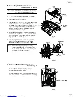
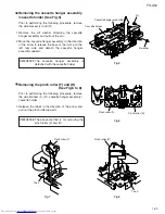
Page 17: ...m Assembly Removing the CL Base Assembly and Tray Refer to Figs 1 to 5 1 Remove the two screws A fastening the CL base assembly from the top of the CD mechanism assembly 2 Move the CL base assembly diagonally upwards as indicated by the arrow to release it from the two hooks a 3 Turn the idle gear in the arrow marked direction from the upper side of the CD mechanism assembly Accordingly the TRAMEC...

Page 18: ... CL base assembly and tray 1 If the TRAMECHA assembly is lowered and it is located out of the PLAY position turn the idle gear in the arrow marked direction so that the hole in the part f of the tray gear meets the hole on the CL base assembly Set the TRAMECHA assembly at the PLAY position 2 Remove the three screws B fastening the TRAMECHA assembly and then remove the TRAMECHA assembly upwards fro...

Page 19: ...th the mechanism board from the back of the mechanism assembly 2 Disconnect the flexible wire from the connector CN601 on the mechanism board 3 Remove the three screws C fastening the mechanism board 4 Unsolder the two points of the part h and one point of the part i of the mechanism board Then remove the mechanism board upwards Note When reinstalling the mechanism board connect the flexible wire ...

Page 20: ...irection from the top of the TRAMECHA assembly so that the pickup assembly is shifted to the reverse side of the T T assembly Move the pickup assembly until the part j of the rack plate in the lower part of the pickup assembly comes out of the CH base assembly 4 Remove the two screws D retaining the shaft of the pickup assembly Next disengage the hook k from the CH base assembly and then remove th...

Page 21: ...while shifting it to the T T side inward so that the part m of the rack plate is positioned as shown in Fig 16 4 Move the pickup assembly to the center position and fasten the shaft with the two screws D Make sure that the part n of the rack plate is correctly engaged with the middle gear 5 After passing the flexible wire coming from the pickup through the opening of the CH base assembly connect i...

Page 22: ...g the side bracket unit R in the direction of the arrow Remove the four screws C attaching the side bracket L in the direction of the arrow 6 7 8 Removing the side bracket L and R load board See Fig 1 to 4 Prior to performing the following procedures turn the mode gear in the direction of the arrow to move each section to the eject position CAUTION The side bracket unit R can be removed even if th...

Page 23: ...sembly cassette holder See Fig 5 The cassette hanger assembly is detached with the cassette holder REFERENCE Prior to performing the following procedure remove the side bracket L R cassette hanger assembly cassette holder Release the tab d in the direction of the arrow and pull out the pinch roller upward 1 Removing the pinch roller F and R See Fig 6 to 8 The above method is for removing the pinch...

Page 24: ...essary 1 2 3 Removing the head assembly head board See Fig 9 and 10 Prior to performing the following procedure remove the side bracket L R cassette hanger assembly cassette holder Remove the belt and sub belt on the bottom of the body Remove the polywasher from the flywheel F and R on top of the body Pull out the flywheel F and R 1 2 3 Removing the flywheel assembly F and R See Fig 11 and 12 Fig ...

Page 25: ...justment and check method 1 CD section 1 Indication of the C1 error 2 Cancel of the C1 error indication To cancel the C1 error indication cut off the power supply While pressing both the POWER key and BACK SKIP key on the main unit turn on the primary power supply FL indication CRC 0 Press the CD OPEN CLOSE key and insert the test disk Press the CD PLAY key The set starts counting and the number o...

Page 26: ...om the back of the cassette mechanism 5 Press the EJECT button on the front side of the cassette mechanism assembly to open the cassette door and then remove the cassette mechanism assembly Head azimuth adjusting screw Reverse side Head azimuth adjusting screw Forward side Playback Recording eraser head Head azimuth adjusting screw Reverse side Head azimuth adjusting screw Forward side Playback Re...

Page 27: ...gnals adjust VR31 so that output level of 10 kHz signals is 2 dB 1 dB of 1 kHz 1 Set a blank cassette tape Type I AC225 and enter the set into the recording pause mode 2 Make sure that the bias frequency at the bias test point Refer on 1 26 board drowing on the head amplifier board is 70 9 kHz 1 Set a blank cassette tape Type I AC225 and enter the set into the recording pause mode 2 After connecti...

Page 28: ...A52 System control board CN706 CN715 CN716 Cassette mechanism assembly Extension code connecting method CD mechanism assembly CD servo control board CN651 System control board CN704 Extension wire QUQ110 1940BJ ...

Page 29: ...mv div 2ms div Fig 1 Approx 3sec pin 25 of IC601 TE Approx 1 8V VREF Tracking error waveform at TOC reading Power ON Power Key Confirm that the Focus error S curve siganl at the pin28 of IC603 is approx 2Vp p Confirm that the siganl from pin24 IC603 R645 is 0V as a accelerated pulse during approx 400ms Automatic tuning of Focus error gain Automatic tuning of Tracking error gain TOC reading Play a ...

Page 30: ... the life of the laser diode has expired the following symptoms wil appear 1 The level of RF output EFM output ampli tude of eye pattern will below Is RF output 1 25 0 22Vp p Replace it NO YES O K 3 Semi fixed resistor on the APC PC board The semi fixed resistor on the APC printed circuit board which is attached to the pickup is used to adjust the laser power Since this adjustment should be perfor...

Page 31: ...1 RxD2 SI2 TxD2 SO2 AD0 AD7 A0 A7 A8 A15 A16 A19 P00 P06 P10 P17 P20 P27 P30 P37 P40 P47 P50 P57 P60 P67 P70 P72 P80 P87 P90 P95 P100 P103 P120 P127 P130 P131 RESET X1 X2 XT1 XT2 VDD VSS TEST RD WR WAIT ASTB ASCK1 SCK1 UART IOE2 BAUD RATE GENERATOR BAUD RATE GENERATOR CLOCKED SERIAL INTERFACE BUS I F PORT0 PORT1 PORT2 PORT3 PORT4 PORT5 PORT6 PORT7 PORT8 PORT9 PORT10 PORT12 PORT13 SYSTEM CONTROL RA...

Page 32: ...output Connected with VDD Not connected PB mute output Not connected Power key input LED control output Buzzer output MD PB output MD reset output System mute output Not connected Not connected Power on control output GND Door position detection UP Door open shut motor control output Door open shut motor control output Door position detection MIDDLE Door position detection DOWN Door open shut moto...

Page 33: ...t detection Function switch key input Destination switch input Function switch key input Cassette key input Current detection GND LED color display control LED color display control Reference power supply 5 V Digital input Digital output Not connected CD digital input CD digital output CD reset LED color display control Not connected Tuner data Tuner data Tuner clock Not connected Not connected No...

Page 34: ...4 P13 AN13 OPEN REST I I I O I O O O I I O I I I I I Connected to GND Not used Pull up B Not used Not used CD emphasis detection CD track No detection CD copy detection GND Power supply Not used Not used Not used Mute output Sub code Q data input from IC651 Not used Sub code Q register clock output to IC651 Kick command data CD control status output to IC801 CD control command clock input from IC8...

Page 35: ...Connected with power supply Flash memory control Connected with external crystal oscillator Connected with external crystal oscillator GND Flag signal input from IC651 Sub code block clock signal input from IC651 RF signal amplitude detection input 2 equalizer switch output 4 equalizer switch output Not used Open door detection Closed door detection 4 DSP current switch output Not used Reset signa...

Page 36: ...RBASS1 RTRE RVRIN RSELO R5 R4 R3 R2 R1 Vref 14 15 16 17 18 19 20 21 22 23 24 25 26 27 28 29 30 31 32 33 34 35 36 1 2 3 4 5 6 7 8 9 10 11 12 13 RVref LVref CONTROL CIRCUIT CONTROL CIRCUIT CCB INTERFACE LOGIC CIRCUIT LOUT LSB LBASS2 LBASS1 LTRE LVRIN LSELO L5 L4 L3 L2 L1 Vref R1 R2 R3 R4 R5 RESLO RVRIN RTRE RBASS1 RBASS2 RSB ROUT RINP RINM ROPOUT VDD CL DI CE VSS LOPOUT LINM LINP LC75345M X IC702 E ...

Page 37: ...pin comprising filters for bass and super bass band Capacitor and resistor connection pin comprising treble band filter Volume input pin Input selector output pin Input signal pin Input signal pin Input signal pin Input signal pin Input signal pin 0 5 x VDD voltage generation block for analog ground Input signal pin Input signal pin Input signal pin Input signal pin Input signal pin Input selector...

Page 38: ...ort clock signal input for sub code Q resister Sub code Q data output Muting input H muting Status signal output Reset signal input L reset Clock signal output MSEL is H 8 4672 MHz MSEL is L 4 2336 MHz Oscillation frequency specification terminal H 33 8688 MHz L 16 9344 MHz TEST2 terminal usually open Traverse drive output Non connect Spindle motor drive signal output Compulsion mode output Spindl...

Page 39: ...ock output Loop filter terminal for VCO Sub code serial output Clock signal input for sub code serial output Connect to ground terminal for oscillation circuit Oscillation circuit input terminal f 16 9344 MHz 33 8688 MHz Oscillation circuit output terminal f 16 9344 MHz 33 8688 MHz Power supply terminal for oscillation circuit Non connect Laser ON signal output H ON General I O port Non connect Fl...

Page 40: ...ts ON OFF BTL AMP 1 input pin BTL AMP 1 input pin For gain adjustment BTL AMP 1 input pin Non inverting side BTL AMP 1 input pin Inverting side BTL AMP 2 input pin Inverting side BTL AMP 2 input pin Non inverting side BTL AMP 2 input pin For gain adjustment BTL AMP 2 input pin External transistor collector PNP connection 5V power supply output External transistor PNP base connection Reset output R...

Page 41: ... AM OSC REG AM RF AFC AM AGC O I O I I I AM Local oscillation Signal output This is a terminal of AM Local oscillation circuit Register value between pin 26 and pin28 besides the frequency width of the input signal AM RF signal input This is an output terminal of voltage for FM AFC This is an AGC voltage input terminal for AM O O I O AM detection output FM detection output Mpx input terminal O O I...

Page 42: ...output port Input output port Data input output Function IF counter signal input IF signal output Not use AM Local OSC signal output FM Local OSC signal input Power suplly VDD 4 5 5 5V When power ON Reset circuit move PLL charge pump output H Local OSC frequency Height than Reference frequency L Low Agreement Height impedance Input for active lowpassfilter of PLL Output for active lowpassfilter of...

Page 43: ... PIN TO GND SHORT PROTECTOR Vcc OUTPUT PIN TO GND SHORT PROTECTOR OVERVOLTAGE SURGE PROTECTOR THERMAL SHUT DOWN LOAD SHORT PROTECTOR OUTOUT PIN TO VCC SHORT PROTECTOR POP NOISE PREVENTION CIRCUIT POWER PREDRIVER POWER PREDRIVER POWER PREDRIVER POWER PREDRIVER IN IN BIAS CIRCUIT STANDBY SW RIPPLE FILTER 1 2 13 14 LA4628 IC801 Power amp 1 Pin layout 2 Block diagram ...

Page 44: ...15 Symbol FB1 VO1 VINA TRIG OC EN1 EN2 GND EN3 FB3 VO3 N C VINB VO2 FB2 Function REG1 feedback voltage input REG1 output voltage Input DC supply voltage Trigger for external SCR crowbar protection Over current warning output REG1 enable input REG2 enable input Analog ground REG3 enable input REG3 feedback voltage input REG3 output voltage Not connected Input DC supply voltage REG2 output voltage R...

Page 45: ... Q14 Q1 R9 Q16 R10 R11 Z1 1 2 3 KIA78S05P T IC803 Regulator Current Limit Output Control Voltage Reference VIN CE VOUT VSS 1 2 3 5 4 Pin No 1 2 3 4 5 Symbol VSS VIN CE NC VOUT Function Ground Supply voltage input Chip enable Non connect Regulated output voltage XC62HR3502P X IC291 Regulator 1 Pin layout 3 Pin function 2 Block diagram ...

Page 46: ...Pre 30k 30k 112k 60k 60k 112k Mute R R ALC Pin No 1 2 3 4 5 6 7 8 9 10 11 12 13 14 15 16 Function CH1 playback amp input Feedback of CH1 playback amp CH1 playback amp output CH1 recording amp input CH1 recording amp output Low cut of ALC Time of ALC GND Vcc Lipple filter Recording amp mute CH2 recording amp output CH2 recording amp input CH2 playback amp output Feedback of CH2 playback amp CH2 pla...

Page 47: ...5 6 7 8 Q5 Q6 Q7 Q8 Q S Q S PARALLEL OUTPUT Q1 15 1 3 2 9 10 QS Q S SERIAL OUTPUT OUTPUT ENABLE STROBE CLOCK DATA Q8 8 STAGE SHIFT REGISTER 8 BIT LATCHES 3 STATE OUTPUTS BU4094BCF X IC333 Shift Store registor 1 2 3 4 5 6 7 8 9 10 GND OUT1 P1 VZ IN1 IN2 VCC1 VCC2 P2 OUT2 Input Output Mode IN1 IN2 OUT1 OUT2 Brake 0 0 0 0 1 0 1 0 0 1 0 1 1 1 0 0 CLOCKWISE COUNTER CLOCKWISE Brake LB1641 IC703 IC704 DC...

Page 48: ... amp output terminal AGC input terminal AGC loop filter capacitor connection terminal AGC output terminal Capacitor connection terminal for HPF amp 3TENV output terminal Capacitor connection terminal for RF enberope detection BDO output terminal Capacitor connection terminal for RF enverope detection OFTR output terminal NRDET output terminal Ground terminal Pin No 17 18 19 20 21 22 23 24 25 26 27...

Page 49: ...1 49 FS A52 M E M O ...

Page 50: ...S A52 Printed in Japan 200203 VICTOR COMPANY OF JAPAN LIMITED AUDIO COMUNICATION BUSINESS DIVISION PERSONAL MOBILE NETWORK BUSINESS UNIT 10 1 1chome Ohwatari machi Maebashi city 371 8543 Japan No 21077 FS A52 ...

Page 51: ...loded view of general assembly and parts list Block No M1 Cassette mechanism assembly and parts list Block No MP CD mechanism assembly and parts list Block No MB Electrical parts list Block No 01 04 Packing materials and accessories parts list Block No M3 M5 FS A52 3 3 3 6 3 8 3 10 3 20 Area suffix J U S A C Canada ...

Page 52: ...FS A52 3 2 M E M O ...

Page 53: ...3 14 33 13 1 74 4 73 75 73 4 9 7 5 6 31 8 A C B C b e c c d 10 4 31 74 108 111 4 12 12 117 116 115 109 38 114 12 12 119 119 111 118 113 110 111 112 e k l m H G n n h j h H d J m 30 34 35 32 101 59 99 100 87 60 78 76 59 77 67 59 39 39 93 51 53 58 57 58 38 49 48 46 43 84 47 43 43 49 61 66 41 42 97 40 39 50 95 80 62 45 52 44 94 63 54 55 44 44 56 83 65 75 82 86 85 82 82 82 81 83 65 102 103 104 105 G K...

Page 54: ...SCREW 1 46 GV40247 001A SPACER 1 47 CD SINGLE MECHA 1 48 GV10080 001A INNER CHASSIS 1 49 QYSBST3006Z T SCREW 4 Item Parts number Parts name Area A Parts list General assembly Q ty Description Block No M1MM 50 QYSBST3006Z T SCREW 1 51 QYSBST3006Z T SCREW 1 52 QYSBSF3010N TAP SCREW 1 53 QYSBSF3010Z SCREW 1 54 GV30201 002A IC HOLDER 1 55 GV30203 001A HEAT SINK 1 56 QYSBSF3012Z SCREW 3 57 GV20153 002A...

Page 55: ...R A 1 109 GV20217 001A GEAR HOLDER B 1 110 GV40191 001A GEAR HOLDER C 1 111 QYSBSF2608Z T SCREW 6 112 WJM0072 001A WIRE 1 113 GV40126 001A PULLEY 1 114 GV30038 001A BELT 1 115 GV40098 001A WORM PULLEY 1 116 GV40097 001A GEAR B 1 117 GV40096 002A GEAR A 1 118 QAR0023 001 MOTOR 1 119 QYSPSP3004Z SCREW 2 120 GV40124 004A SPACER 2 KI901 QLD0184 001 LCD MODULE 1 LCD ...

Page 56: ...FS A52 3 6 3 4 5 6 7 8 9 9 9 9 9 10 11 2 EM 60L FL 721 Grease Loading mecha Caccette mecha Cassette mechanism assembly and parts list Block No M M M P ...

Page 57: ...cription Block No MPMM 1 BDL1141 001M C MECHA UNIT 1 2 F513 884 HEAD BLOCK 1 3 FF19Y MAIN BELT 1 4 UJ16F 11 WASHER 1 5 F522 064 FLYWHEEL 1 6 FR26K FLYWHEEL 1 7 F514 129 PINCH ROLLER 1 8 F514 130 PINCH ROLLER 1 9 KG194 28 TT SCREW 1 2 6X4 10 FF18W F R BELT 1 11 KG194 34 TT SCREW 1 2 0X4 ...

Page 58: ...echanism assembly and parts list Block No M M M B CD servo board 21 22 22 16 6 11 12 7 9 15 15 13 17 18 10 10 4 17 18 2 5 3 14 23 24 23 24 1 20 7 2 0 2 mm 13 8 0 1 mm 17 19 8 14 13 5 3 21 BACK SIDE 20 BACK SIDE UD 24H2 EM 30L LEN 320M ...

Page 59: ...002A RACK PLATE 1 8 QYSPSGT1735M MINI SCREW 2 9 E406777 002SM C D SHAFT 1 10 LV41741 001A SPECIAL SCREW 2 11 LV31744 001A P S SPRING 1 12 QYSPSGT1425M TAP SCREW 1 13 LV42350 001A T T ASSY 1 14 QAR0175 001 SP MOTOR 1 15 VKZ4743 001 SPECIAL SCREW 2 16 LVB30008 001A FPC 1 17 LV41424 001A SPECIAL SCREW 3 18 LV41659 001A INSULATOR 2 19 LV41659 002A INSULATOR 1 20 LV10503 002A TRAY 1 21 LV32650 001A CL ...

Page 60: ...F CAPACITOR 10MF 5 50V C1402 QEKC1CM 107Z E CAPACITOR 100MF 20 16V C1501 EETC1CM 107ZJC E CAPACITOR C1502 QCFB1HZ 105Y C CAPACITOR 1 0MF 80 20 C1601 EETC1CM 107ZJC E CAPACITOR C1602 QCFB1HZ 104Y C CAPACITOR 10MF 80 20 C1701 QETN1CM 107Z E CAPACITOR 100MF 20 16V C1704 QDGB1HK 102Y C CAPACITOR C1705 QDGB1HK 102Y C CAPACITOR C1706 QENC1HM 106Z NP E CAPACITOR 10MF 20 50V C1707 QENC1HM 106Z NP E CAPACI...

Page 61: ... 1 0K 5 1 4W R1801 QRE141J 681Y C RESISTOR 680 5 1 4W R1802 QRE141J 681Y C RESISTOR 680 5 1 4W R1803 QRE141J 681Y C RESISTOR 680 5 1 4W R1804 QRE141J 681Y C RESISTOR 680 5 1 4W R1805 QRE141J 472Y C RESISTOR 4 7K 5 1 4W R1806 QRE141J 272Y C RESISTOR 2 7K 5 1 4W R1807 QRE141J 681Y C RESISTOR 680 5 1 4W R1901 QRE141J 912Y C RESISTOR 9 1K 5 1 4W R1902 QRE141J 122Y C RESISTOR 1 2K 5 1 4W R2601 QRE141J ...

Page 62: ...OR C2227 QETC1HM 475Z E CAPACITOR 4 7MF 20 50V C2229 QEKC1HM 475Z E CAPACITOR 4 7MF 20 50V C2230 QEKC1HM 475Z E CAPACITOR 4 7MF 20 50V C2231 EEKC1CM 226ZJC E CAPA I M C2404 NCB31HK 103X C CAPACITOR C2453 NCB31HK 103X C CAPACITOR C2502 EETC1CM 107ZJC E CAPACITOR C2600 NCB31CK 823X C CAPACITOR C2601 NCB31CK 823X C CAPACITOR C2602 NCB31CK 823X C CAPACITOR C2603 NCB31CK 823X C CAPACITOR C2604 NCB21HK ...

Page 63: ...875 GR X TRANSISTOR Q2707 KTC3875 GR X TRANSISTOR Q2708 KTC3875 GR X TRANSISTOR Q2709 KTC3875 GR X TRANSISTOR Q2710 KTC3875 GR X TRANSISTOR Q2711 KTC3875 GR X TRANSISTOR Q2712 KTC3875 GR X TRANSISTOR Q2713 KTC3875 GR X TRANSISTOR Q2714 KTC3875 GR X TRANSISTOR Q2715 KTC3875 GR X TRANSISTOR Q2716 KTC3875 GR X TRANSISTOR Q2717 KTC3875 GR X TRANSISTOR Q3101 DTC114TKA X TRANSISTOR 70U 12U Q3201 DTC114T...

Page 64: ...OR R2209 NRSA63J 182X MG RESISTOR R2210 NRSA63J 122X MG RESISTOR R2211 NRSA63J 682X MG RESISTOR R2225 QRE141J 222Y C RESISTOR 2 2K 5 1 4W R2226 QRE141J 222Y C RESISTOR 2 2K 5 1 4W R2227 QRE141J 182Y C RESISTOR 1 8K 5 1 4W R2228 QRE141J 472Y C RESISTOR 4 7K 5 1 4W R2229 NRSA63J 752X MG RESISTOR R2230 NRSA63J 752X MG RESISTOR R2231 QRE141J 182Y C RESISTOR 1 8K 5 1 4W R2232 QRE141J 182Y C RESISTOR 1 ...

Page 65: ...RESISTOR R3206 NRSA63J 332X MG RESISTOR R3207 NRSA63J 123X MG RESISTOR R3208 NRSA63J 562X MG RESISTOR R3209 NRSA63J 102X MG RESISTOR R3210 NRSA63J 272X MG RESISTOR R3211 NRSA63J 363X MG RESISTOR R3212 NRSA63J 222X MG RESISTOR R3216 NRSA63J 102X MG RESISTOR R3221 NRSA63J 223X MG RESISTOR R3301 NRS181J 221X MG RESISTOR VCC R3303 NRSA63J 393X MG RESISTOR R3304 NRS181J 101X MG RESISTOR VCC R3305 NRSA6...

Page 66: ... E CAPA I M C 51 EEKC1HM 105ZJC E CAPACITOR C 52 QFVJ1HJ 274Z MF CAPACITOR 27MF 5 50V C 53 EETC1CM 226ZJC E CAPA I M C 54 NCB21HK 473X C CAPACITOR C 57 NCB21HK 102X C CAPACITOR C 58 NCB21HK 473X C CAPACITOR C 59 NCB21HK 102X C CAPACITOR CF 1 QAX0677 001Z C FILTER CF 2 QAX0677 001Z C FILTER CF 3 QAX0610 001Z C DISCRIMINATOR CN 1 QGF1205F1 09 CONNECTOR D 1 1SS133 T2 SI DIODE IM D 2 1SS133 T2 SI DIOD...

Page 67: ...CAPACITOR C 816 NCB20JK 155X C CAPACITOR C 817 NCF21CZ 105X C CAPACITOR C 818 NCF21CZ 105X C CAPACITOR C 821 NCF21CZ 105X C CAPACITOR C 822 QERF1AM 227Z E CAPACITOR 220MF 20 10V C 861 NCB31HK 102X C CAPACITOR C 862 NCB31HK 102X C CAPACITOR C 863 NCB31HK 272X C CAPACITOR C 864 NCB31HK 272X C CAPACITOR CN601 QGF1037F1 15W CONNECTOR PICK UP TR MECH CN605 QGF1016F2 04W CONNECTOR CD TEXT CN606 QGF1016F...

Page 68: ...J 102X MG RESISTOR R 678 NRSA63J 102X MG RESISTOR R 679 NRSA63J 102X MG RESISTOR R 682 NRSA63J 102X MG RESISTOR R 683 NRSA63J 105X MG RESISTOR R 685 NRSA63J 683X MG RESISTOR R 801 NRSA63J 272X MG RESISTOR R 802 NRSA63J 152X MG RESISTOR R 803 NRSA63J 472X MG RESISTOR R 804 NRSA63J 103X MG RESISTOR R 805 NRSA63J 123X MG RESISTOR R 808 NRSA63J 183X MG RESISTOR R 809 NRSA63J 152X MG RESISTOR R 811 NRS...

Page 69: ...FS A52 3 19 M E M O ...

Page 70: ...FS A52 3 20 Packing materials and accessories parts list Block No M M M 3 Block No M M M 5 P3 P5 P4 P1 P2 A1 A10 P12 P10 P11 P8 P6 P7 P6 A14 A13 P7 A12 A11 P9 ...

Page 71: ...P 11 GV40168 004A SHEET 1 P 12 GV30229 001A CARTON SPACER 1 Item Parts number Parts name Area A Parts list Accessories Q ty Description Block No M5MM A 1 EWP503 001C ANT WIRE 1 A 2 QAL0014 001 AM LOOP ANT 1 A 3 GVT0071 002A INST BOOK C 1 ENG FRE GVT0071 001B INST BOOK J 1 ENG A 4 QMPE180 183 JN POWER CORD A 1 A 5 RM SFSA52J REMOCON 1 A 6 BATTERY 2 A 7 BT 51028 1 J REGIST CAR J 1 A 8 YU20333 SAFETY...

Page 72: ...PEN REST FM FM SM SM TRD FOD ECM ECS TVD DQSY SBCK SUBC SRDATA LRCK BCLK A C B D E F LD MD OFT BDO ARF RFENV TBAL FBAL FE TE GCTL RFDET RESET STAT DMUTE SUBQ SQCK BLKCK MLD MDATA MCLK FLAG IREFx4 TX OUTL OUTR RESET MCS KCMND MSTAT MRDY KCLK CDCOPY CDTNO CDEMP CDINDEX TXDO RXDO IC RESET to FLASH MICON DIGITAL OUT CN705 IC702 FUCTION VOL AHB BUZZER PIN FKEY1 FKEY2 CN709 J2003 CN701 CN744 CN743 CN711...

Page 73: ... GR X 10K 47K QQL244K 100Z QQR0621 001Z 10K 10K 10K 10K GP1FA550TZ NQR0428 002X 470P 15K 4 7K 4 7K 10K 1 8K 1 8K 1 8K 1 8K QGB2024J1 20S QGB2024K1 20S QGF1016F1 14 3 3K 5 6K 1K 1K 1K 100P 100P 2 2K 0 012 KTC3875 GR X 39K 39K 0 01 QGF1016F1 14 GP1UM271XK 1K 1K 1 2K 1 5K 2 2K 2 7K 3 9K 1K 1K 1 2K 1 5K 2 2K 2 7K QGB2510J1 12 2 2K 2 2K 2 2K 10K 100P 100P 10K 0 01 3 9K 100K 82K 390K 82K KTC3875 GR X 0 ...

Page 74: ...8 R1707 D1012 C1401 Q1702 Q1703 C1706 C1707 D1603 C1710 C1005 R1615 C1402 C1301 D1301 R1301 C1018 F1003 F1004 CN804 L4909 0 022 0 022 IN5401 TM 0 1 0 1 IN5401 TM IN5401 TM IN5401 TM KRA101M T QQR0779 001Z 1N5401 TM QQR1145 001 2SC2785 FE T QQR0779 001Z QGB2510K2 12 QGB2510K2 12 QQR0621 001Z KTB772 Y 2SC2785 FE T QQR0621 001Z 2 7K 330 680 150 150 220P 3 9K 3 9K 0 01 KIA78S05P T 4 7K 4 7K 10 35 10 3...

Page 75: ...0 022 0 1 25 QGF1016F2 08W DTC114EUA X 82k 180k 0 001 0 001 150 DTC114EUA X 15p 47k 47k 1k 22p MN662790RSC 1k 1k 4 7 1k 470p 1p QAX0599 001Z 1p DA204U X 0 01 50 100 10 0 33 16 0 1 25 1k 1M HFW15R 1STE1 DTA114EKA x MA112 X 10 2700p 680 560 680 2700p NI 560 NI TC7S00F X 1000p 1000p NI 5 6k 3 3k QGF1016F2 19W 1 16 CSTS8 38MG 1 16 680k NI QGA2001F2 02X 47k NQR0288 004X NQR0288 004X TK11235BMC X 1k 1k ...

Page 76: ...C3209 R3210 C3301 C3305 C3304 C3206 R3375 C3376 C3113 C3102 R3303 R3219 R3116 C3302 C3103 C3319 C3316 C3310 C3314 C3313 R3313 C3374 C3371 C3105 SW6 SW4 SW5 SW1 SW2 C3205 220 2 4K 2 4K QVP0008 203Z 2SC2412K RS 2SA952 LK 5 6K MA3051 M 1SR139 400 T2 0 033 47 BU4094BCF 330P 0 033 10K 22K 22K 5 6K 36K 12K 100 330P QQR1118 001 BA3126N 4 7 25 3 9K 1 8K 12K QVP0008 103Z 3 3K 2SB562 C 4 7K DTC124EKA 2 2K 4...

Page 77: ...8 R35 C37 R18 C41 C33 R19 R20 R22 C19 C4 C1 R13 R40 C3 R6 R60 C60 R1 100 10 0 27 QAX0610 001Z VCF2L3B 105Z 470P 0 001 1 50 0 001 0 001 LC72136N 0 047 0 1 3 3k 68 1 4W F RES 100 10 12P 12P 4 7K 0 001 0 047 12P 10K 3 3K 5 6K 10K 0 047 150P 10K LA1838 VCF2L3B 105Z 10 16 56K 10 16 22 16 56K 10K 0 022 1 50 1K 100 10 1K 150P 150P QGF1205F1 09 0 47 50 1 2K QQR0793 001 1SS133 T2 1SS133 T2 22 16 0 001 1000...

Page 78: ...A B C D E F G 1 2 3 4 5 2 7 FS A52 Main board Printed circuit boards ...

Page 79: ...FS A52 FS A52 A B C D E F G 1 2 3 4 5 2 8 Power amplifier board ...

Page 80: ...1 TP2 X251 SW102 C273 R276 R265 D251 R264 IC652 C654 K651 R655 R656 C668 C254 C291 C605 C606 C608 C610 C611 C612 C617 C622 C624 C631 C651 C652 C653 C657 C658 C661 C663 C665 C667 C673 C676 C677 C678 C679 C801 C802 C812 C815 C816 C821 C822 CN605 CN606 CN651 R291 IC601 IC651 K655 K656 K657 K658 M851 M852 Q631 R254 R255 R256 R257 R258 R260 R271 R272 R281 R282 R283 R284 R285 R603 R604 R293 R611 R613 R6...

Page 81: ...A B C 1 2 3 4 5 FS A52 2 10 Tuner board ...

Page 82: ...A B C 1 2 3 4 5 FS A52 2 11 CN601 MT601 MT602 S602 S601 Traverse mechanism board Forward side Reverse side Traverse mechanism board SW1 SW2 SW3 SW4 SW5 P1 D1 IC1 CN1 SW6 T01 Cassette switch board ...

Reviews: