background image

SP-5000M-PMCL / SP-5000C-PMCL 

- 40 - 


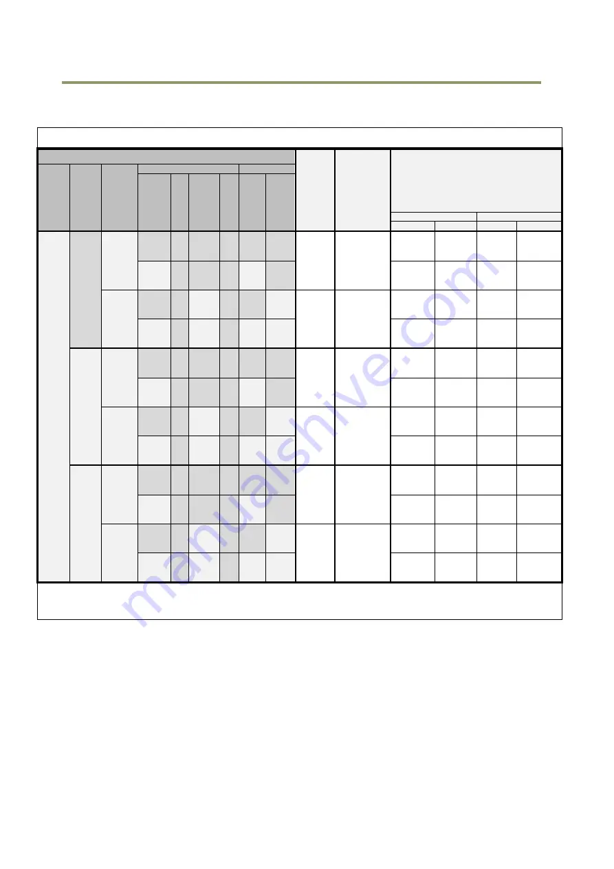
Table 28.      Continuous Trigger / Vertical timing          1X4

1Y (2/3) 

Camera Settings 


(E)


(F)


T

a

p


Ge
o

m

e

tr

y


Cam

e

ra


L

ink
 

P

ixel Cloc

k


F

ra

m

e


P

e

rio

d


(T

y

p

.)


ROI 

Binning 

Frame 

Rate 

Exposure 

Time 

(Max.)


Exposure Active    End 

to 

FVAL Active Start


W
idt
h


Of
fse

X


Heig

h

Of
fse

Y


Hor

iz

o

n

ta

V

e

rtic
a

[Unit: 

Hz]


[Unit: us]


[Unit: Line] 

[Unit: us] 

Max 

Min 

Max 

Min 

1X4 

-1Y 

82.3 

MHz 

16393 

2560 

2048 

(Off) 

(Off) 

60.97 

16393 - 100 

16293 

11.0 

to 

12.0 

5.1 

to 

6.1 

86.5 

to 

94.2 

40.3 

to 

48.1 

1280 

2048 

(On) 

(Off) 

10.6 

to 

11.6 

4.7 

to 

5.7 

83.1 

to 

90.9 

37.0 

to 

44.7 

8197 

2560 

1024 

(Off) 

(On) 

121.95 

8197 - 100 

8097 

11.0 

to 

12.0 

5.1 

to 

6.1 

86.5 

to 

94.2 

40.3 

to 

48.1 

1280 

1024 

(On) 

(On) 

10.6 

to 

11.6 

4.7 

to 

5.7 

83.1 

to 

90.9 

36.9 

to 

44.7 

75.4 

MHz 

17883 

2560 

2048 

(Off) 

(Off) 

55.90 

17883 - 100 

17783 

11.6 

to 

12.6 

4.9 

to 

5.9 

99.3 

to 

107.6 

41.8 

to 

50.1 

1280 

2048 

(On) 

(Off) 

11.2 

to 

12.2 

4.5 

to 

5.5 

95.9 

to 

104.3 

38.4 

to 

46.9 

8942 

2560 

1024 

(Off) 

(On) 

111.78 

8942 - 100 

8842 

11.6 

to 

12.6 

4.9 

to 

5.9 

99.2 

to 

107.7 

41.7 

to 

50.2 

1280 

1024 

(On) 

(On) 

11.2 

to 

12.2 

4.5 

to 

5.5 

95.9 

to 

104.4 

38.4 

to 

46.9 

61.7 

MHz 

21858 

2560 

2048 

(Off) 

(Off) 

45.73 

21858 - 100 

21758 

12.8 

to 

13.8 

4.4 

to 

5.4 

133.7 

to 

144.1 

45.6 

to 

56.0 

1280 

2048 

(On) 

(Off) 

12.5 

to 

13.5 

4.0 

to 

5.0 

130.4 

to 

140.8 

42.3 

to 

52.7 

10929 

2560 

1024 

(Off) 

(On) 

91.45 

10929 - 100 

10829 

12.8 

to 

13.8 

4.4 

to 

5.4 

133.8 

to 

144.1 

45.6 

to 

56.0 

1280 

1024 

(On) 

(On) 

12.5 

to 

13.5 

4.0 

to 

5.0 

130.4 

to 

140.8 

42.3 

to 

52.7 

[Note]    In 

1X4-1Y Tap Geometry, 

“Exposure Active End to FVAL Active Start” period varies depending on the 

exposure time setting. When the exposure time is set at “10”, it is the maximum period and if the exposure time is 
incremented by 1 us, it is decreased.   

Summary of Contents for SP-5000M-PMCL

Page 1: ...1046E 1305 Spark Series SP 5000M PMCL SP 5000C PMCL 5M CMOS Digital Progressive Scan Monochrome and Color Camera Document Version Ver 1 1 SP 5000 PMCL_Ver 1 1_Oct2013 User Manual ...

Page 2: ...CC This equipment has been tested and found to comply with the limits for a Class B digital device pursuant to Part 15 of the FCC Rules These limits are designed to provide reasonable protection against harmful interference in a residential installation This equipment generates uses and can radiate radio frequency energy and if not installed and used in accordance with the instructions may cause h...

Page 3: ...oducts known as China RoHS The table shows contained Hazardous Substances in this camera mark shows that the environment friendly use period of contained Hazardous Substances is 15 years 嶷勣廣吭並 嗤蕎 嗤墾麗嵎賜圷殆兆各式根楚燕 功象嶄鯖繁酎慌才忽佚連恢匍何〆窮徨佚連恢瞳麟半陣崙砿尖一隈〇 云恢瞳ゞ 嗤蕎 嗤 墾麗嵎賜圷殆兆各式根楚燕 泌和 桟隠聞喘豚 窮徨佚連恢瞳嶄根嗤議嗤蕎嗤墾麗嵎賜圷殆壓屎械聞喘議訳周和音氏窟伏翌 亶賜融延 窮徨佚連恢瞳喘薩聞喘乎窮徨佚連恢瞳音氏斤桟廠夛撹冢嶷麟半 賜斤児繁附 夏恢夛撹冢嶷鱒墾議豚 方忖仝15々葎豚 15定 ...

Page 4: ...oducts known as China RoHS The table shows contained Hazardous Substances in this camera mark shows that the environment friendly use period of contained Hazardous Substances is 15 years 嶷勣廣吭並 嗤蕎 嗤墾麗嵎賜圷殆兆各式根楚燕 功象嶄鯖繁酎慌才忽佚連恢匍何〆窮徨佚連恢瞳麟半陣崙砿尖一隈〇 云恢瞳ゞ 嗤蕎 嗤 墾麗嵎賜圷殆兆各式根楚燕 泌和 桟隠聞喘豚 窮徨佚連恢瞳嶄根嗤議嗤蕎嗤墾麗嵎賜圷殆壓屎械聞喘議訳周和音氏窟伏翌 亶賜融延 窮徨佚連恢瞳喘薩聞喘乎窮徨佚連恢瞳音氏斤桟廠夛撹冢嶷麟半 賜斤児繁附 夏恢夛撹冢嶷鱒墾議豚 方忖仝15々葎豚 15定 ...

Page 5: ...mera Link pixel clock frequency 15 5 3 Digital IN OUT interface 16 5 3 1 Line Selector 16 5 3 2 Line Source 16 5 3 3 Line Mode 16 5 3 4 Line Inverter 16 5 3 5 Line Status 16 5 3 6 Line Format 17 5 3 7 GPIO 17 5 3 7 1 Basic block diagram 17 5 3 7 2 Input and output matrix table 18 5 4 Pulse Generator 18 5 4 1 Clock Pre scaler 19 5 4 2 Pulse Generator Selector 19 5 4 3 Pulse Generator Length 20 5 4 ...

Page 6: ... operation Timed Exposure Mode Trigger Mode OFF 49 7 5 Timed mode EPS operation 49 7 5 1 If Overlap setting is OFF 50 7 5 2 If Overlap setting is Readout 50 7 6 Trigger width mode PWC 51 7 6 1 If Overlap setting is OFF 51 7 6 2 If Overlap setting is Readout 52 7 7 RCT mode 53 7 8 PIV Particle Image Velocimetry 54 7 9 Sequence Mode 55 7 9 1 Video send mode 55 7 9 2 Sequence mode 55 7 9 3 Sequence m...

Page 7: ...ication setting 77 2 Protocol Short ASCII Command 77 2 1 Transmit the setting command to camera 77 2 2 Transmit the request command to camera 77 2 3 Switching baud rate between PC and camera 77 2 4 Command list Short ASCII command 78 2 4 1 GenCP Bootstrap Register 78 2 4 2 Technology Specific Bootstra Register 78 2 4 3 Device Control 79 2 4 4 Image Format Control 79 2 4 5 Acquisition Control 80 2 ...

Page 8: ...ied to the camera through the Camera Link cable s Because the power requirements of the camera exceed the amount of power which can be provided over a single PoCL connection power must be supplied via both Camera Link cables in order to utilize the PoCL capabilities If you plan to use this function please be sure that the frame grabber board you are using also complies with this specification Alte...

Page 9: ...A full pixel readout or partial scan readout mode can be selected depending on applications The readout format is available for 10 tap 8 tap 4 tap or 2 tap output The SP 5000M PMCL and SP 5000C PMCL have various comprehensive functions needed for automated optical inspection applications such as solid state device inspection or material surface inspection They incorporate video processing function...

Page 10: ...L 10 μs 1 100 000 to 8 seconds exposure control in 1 μs step Auto exposure control Timed and trigger width exposure control RCT and PIV trigger modes for specific applications ALC control with combined function of AGC Auto Shutter and Auto Iris Various pre processing circuits are provided Programmable LUT Gamma correction from 0 45 to 1 0 Shading correction Bayer white balance with manual or one p...

Page 11: ...nd Full config Note 2 Mounting holes M3 depth 5mm for fixing the camera to the tripod base or direct installation Note 3 1 Note Rear protrusion on C mount lens must be less than 10 0 mm 2 Note When a Camera Link cable is connected to the camera please do not excessively tighten screws by using a driver The Camera Link receptacle on the camera might be damaged For security the strength to tighten s...

Page 12: ...ing information Amber Power connected initiating This light goes OFF after initiating Steady green Camera is operating in Continuous mode Flashing green The camera is receiving external triggering Note The interval of flashing does not correspond with external trigger duration Fig 2 Rear panel ...

Page 13: ...ive Note 2 Factory default setting is trigger input Note 3 See page 6 for notes about power options for these cameras 5 1 2 Camera Link Connector 5 1 2 1 Figure Type 26 pin Mini Camera Link connector Honda HDR EC26FYTG2 SL See page 6 for notes about Power over Camera Link PoCL options for this camera Fig 4 Camera Link connector 1 14 13 26 Pin no Signal Remarks 1 GND 2 DC input 12V 24V note 3 3 GND...

Page 14: ...nput 10 23 CC1 Reserved 11 24 N C 12 25 N C 13 14 Shield Power Return Camera Link connector 2 Pin No In Out Name Note 1 26 Power Power 2 15 O Y_OUT0 Data output 3 16 O Y_OUT1 4 17 O Y_OUT2 5 18 O Y_Clk Clock for CL 6 19 O Y_OUT3 Data output 7 20 I N C 8 21 O Z_OUT0 Data output 9 22 I Z_OUT1 10 23 Z_OUT2 11 24 Z_Clk Clock for CL 12 25 Z_OUT3 Data output 13 14 Shield Power Return 5 1 3 AUX Standard ...

Page 15: ...in connector factory option Type HIROSE 10 Pin Connector 3260 10S3 55 Table 4 10 pin pin configuration option No I O Name Note 1 O Video Signal Video Iris Lens 2 O Power DC 12V Video Iris Lens 3 NC 4 NC 5 GND 6 O DC IRIS DAMP DC Iris 7 O DC IRIS DAMP DC Iris 8 O DC IRIS DRIVE DC Iris 9 O DC IRIS DRIVE DC Iris 10 GND 5 1 5 AUX Type 3 HIROSE 10 Pin connector factory option HIROSE 10 Pin Connector 32...

Page 16: ...TxIN 25 FVAL FVAL FVAL FVAL FVAL Port I0 TxIN 26 DVAL DVAL DVAL Tap 1 D0 Tap 4 D0 Port I1 TxIN 23 Exposure Active Exposure Active Exposure Active Tap 1 D1 Tap 3 D7 SP 5000M C PMCL Camera Link Configuration Camera Link port bit GenICam Tap Geometry D i g i t a l I O 1 Port Base Medium Full 80bit Full 2Tap 12bit 4Tap 12bit 8 Tap 8bit 8 Tap 10bit 10 Tap 8bit 1X2 1Y 1X4 1Y 1x8 1Y 1X8 1Y 1X10 1Y Port D...

Page 17: ...p10 D7 Port K7 TxIN 23 Exposure Active Tap 8 D1 Tap10 D4 SP 5000M C PMCL D i g i t a l I O 2 2 2 Port Camera Link Configuration Camera Link port bit GenICam Tap Geometry Note 1 In this table not all tap geometry items are described For instance 1X4 1Y shows only 12 bit In case of 10 bit upper 2 bits D10 and D11 are not used and in case of 8 bit upper 4 bits D8 through D11 are not used 2 Please che...

Page 18: ...urce item Description Low Connect Low Level signal to line item selected in Line Selector Default setting High Connect High Level signal to line item selected in Line Selector Frame Trigger Wait Connect Frame Trigger Wait signal to line item selected in Line Selector Frame Active Connect Frame Active signal to line item selected in Line Selector Exposure Active Connect Exposure Active signal to li...

Page 19: ... together with a PWC trigger 5 3 7 1 Basic block diagram The basic block diagram is as follows In the SP 5000 PMCL the pixel clock is 48 MHz Soft Trigger LVAL IN FVAL IN Exposure Active Frame Trigger Wait Frame Active GPIO 4 TTL IN 1 GPIO 7 CL CC1 GPIO 10 TTL IN2 GPIO 11 LVDS IN Pixel Clock Cross Pont Switch 12 bit Counter INV INV INV N NAND INV Non INV Pulse Generator 20 bit counter x 4 CLR Sel B...

Page 20: ...er Source Line Selector Pulse Generator Selector Trigger Source Frame Start Line 1 12P TTL Out Line 8 TTL 2 Out Trigger Selector Pulse Generator Clear Source Line Source Line 9 TTL 3 Out NAND 1 In 1 NAND 1 In 2 NAND 2 In 1 NAND 2 In 2 Pulse Generator 0 Pulse Generator 1 Pulse Generator 2 Pulse Generator 3 Note In the above table TTL 2 IN LVDS IN TTL 2 Out and TTL 3 Out are available only if AUX Ty...

Page 21: ... operating in free running mode However based on the above default settings Length 1 Start Point 0 and End Point 1 Pulse Generator stops at High output Therefore if Start Point 0 and End Point 1 are configured Length should be 2 as the minimum active width Trigger Selector item Description Pulse Generator 0 If Pulse Generator 0 is selected Length Start Point End Point Repeat Count Clear Source Cle...

Page 22: ...ingly an active pulse which has a start point and end point can be output repeatedly However if Repeat Count is set to 0 it works as free running counter 5 4 7 Pulse Generator Clear Activation Set the clear conditions of clear count pulse for the selected pulse generator 5 4 8 Pulse Generator Clear Sync Mode Set the count clear method for the selected pulse generator In case of Async Mode if the c...

Page 23: ...ut Pulse Generator Clear Source In Example 1 Clear Activation Rising Edge Clear Sync Mode Async Mode Clear Inverter False Example 2 Clear Activation Rising Edge Clear Sync Mode Sync Mode Clear Inverter False Pulse Generator Output Pulse Generator Clear Source In 0 Pulse Generator Length 0 Clear Note Repeat Count is also reset ...

Page 24: ...the selected pulse generator PulseGenerator0 Out Connect Pulse Generator 0 output to Clear Source for the selected pulse generator PulseGenerator1 Out Connect Pulse Generator 1 output to Clear Source for the selected pulse generator PulseGenerator2 Out Connect Pulse Generator 2 output to Clear Source for the selected pulse generator PulseGenerator3 Out Connect Pulse Generator 3 output to Clear Sou...

Page 25: ...ulse Generator End Point 1 to 1048575 Pulse Generator End Point ms Clock Source Clock Pre scaler 1 x Pulse Generator End Point Pulse Generator pulse width ms Pulse Generator End Point ms Pulse Generator Start Point ms Pulse Generator Repeat Count 0 to 255 Pulse Generator Clear Activation Clear Mode for the Pulse Generators Off High Level Low level Rising Edge Falling Edge Pulse Generator Clear Syn...

Page 26: ...ensor layout The CMOS sensors used in the SP 5000M PMCL and SP 5000C PMCL have the following pixel layout 6 1 1 Monochrome sensor Fig 10 Monochrome sensor layout 6 1 2 Bayer sensor Fig 11 Color sensor layout 2560 Pixels 2048 Pixels F Pixel 0 0 2560 Pixels 2048 Pixels F Pixel 0 0 ...

Page 27: ...2 tap readout system specified in GenICam Tap Geometry and it outputs as the following Width 2560 Pixel 1280 Pixel x 2 Taps Height 2048 Pixel X5120 Y1 X5120 Y3840 X4 Y1 X4 Y2048 X3 Y1 X3 Y2048 X2 Y1 X2 Y2048 X5 Y1 X5 Y2048 X6 Y1 X6 Y2048 X7 Y1 X7 Y2048 X8 Y1 X8 Y2048 X2053 Y1 X2553 Y2048 X2054 Y1 X2554 Y2048 X2055 Y1 X2555 Y2048 X2056 Y1 X2556 Y2048 X2057 Y1 X2557 Y2048 X2058 Y1 X2558 Y2048 X2059 ...

Page 28: ...047 X2560 Y2048 X1 Y1 X1 Y2 X1 Y2047 X1 Y2048 Tap 1 Tap 2 Pixel 0 0 Step Y 1 Step X 4 Tap 2 Tap 2 Fig 13 1X4 1Y output format 6 2 3 1X8 1Y 1X8 1Y is an 8 tap readout system and outputs as follows Width 2560 Pixel 1280 Pixel x 2 Taps Height 2048 Pixel X5120 Y1 X5120 Y3840 X4 Y1 X4 Y2048 X3 Y1 X3 Y2048 X2 Y1 X2 Y2048 X5 Y1 X5 Y2048 X6 Y1 X6 Y2048 X7 Y1 X7 Y2048 X8 Y1 X8 Y2048 X2053 Y1 X2553 Y2048 X2...

Page 29: ... X2559 Y2048 X2056 Y1 X2056 Y2 X2560 Y2047 X2560 Y2048 X1 Y1 X1 Y2 X1 Y2047 X1 Y2048 Tap 1 Tap 4 Pixel 0 0 Step Y 1 Step X 10 Tap 6 Tap 8 Tap 2 Tap 5 Tap 3 Tap 7 Tap 9 Tap 10 Fig 15 1X10 1Y Output format 6 3 Output timing and output image 6 3 1 Horizontal timing The horizontal frequency is changed by setting the Tap Geometry In the SP 5000M PMCL and SP 5000C PMCL H binning is available but the hor...

Page 30: ...idth Offset X Height Offset Y Hori zont al Verti cal Unit Clock Unit kHz Unit us 1X10 1Y 82 3 MHz 2560 0 2048 0 1 1 a 283 to 286 290 763 to 287 713 3 439 to 3 476 b 284 56 289 169 3 458 1280 0 2048 0 2 1 a 283 to 286 290 763 to 287 713 3 439 to 3 476 b 284 56 289 169 3 458 2560 0 1024 0 1 2 a 283 to 286 290 763 to 287 713 3 439 to 3 476 b 284 56 289 169 3 458 1280 0 1024 0 2 2 a 283 to 286 290 763...

Page 31: ...82 3 MHz 2560 0 2048 0 1 Off 1 Off 320 4 to 7 0 1280 0 2048 0 2 On 1 Off 160 164 to 167 0 2560 0 1024 0 1 Off 2 On 320 4 to7 0 1280 0 1024 0 2 On 2 On 160 164 to167 0 75 4 MHz 2560 0 2048 0 1 Off 1 Off 320 4 to 7 0 1280 0 2048 0 2 On 1 Off 160 164 to 167 0 2560 0 1024 0 1 Off 2 On 320 4 to 7 0 1280 0 1024 0 2 On 2 On 160 164 to 167 0 61 7 MHz 2560 0 2048 0 1 Off 1 Off 320 3 to 5 0 1280 0 2048 0 2 ...

Page 32: ...639 3 958 1280 0 a b 0 2 On 2 On a 324 to 327 253 969 to 3 937 to 3 974 b 325 71 252 639 3 958 75 4 MHz 2560 0 a b 0 1 Off 1 Off a 324 to 327 232 806 to 230 670 4 295 to 4 335 b 325 29 231 882 4 313 1280 0 a b 0 2 On 1 Off a 324 to 327 232 806 to 230 670 4 295 to 4 335 b 325 29 231 882 4 313 2560 0 a b 0 1 Off 2 On a 324 to 327 232 806 to 230 670 4 295 to 4 335 b 325 29 231 882 4 313 1280 0 a b 0 ...

Page 33: ... 2560 0 2048 0 1 Off 1 Off 640 3 to 6 0 1280 0 2048 0 2 On 1 Off 320 323 to 326 0 2560 0 1024 0 1 Off 2 On 640 3 to 6 0 1280 0 1024 0 2 On 2 On 320 323 to 326 0 75 4 MHz 2560 0 2048 0 1 Off 1 Off 640 3 to 6 0 1280 0 2048 0 2 On 1 Off 320 323 to 326 0 2560 0 1024 0 1 Off 2 On 640 3 to 6 0 1280 0 1024 0 2 On 2 On 320 323 to 326 0 61 7 MHz 2560 0 2048 0 1 Off 1 Off 640 4 to 7 0 1280 0 2048 0 2 On 1 O...

Page 34: ... 2 On 2 On a 643 to 646 127 972 to 127 378 7 814 to 7 851 b 644 57 127 632 7 835 75 4 MHz 2560 0 2048 0 1 Off 1 Off a 643 to 646 117 308 to 116 861 8 525 to 8 557 b 644 29 117 073 8 542 1280 0 2048 0 2 On 1 Off a 643 to 646 117 308 to 116 861 8 525 to 8 557 b 644 29 117 073 8 542 2560 0 1024 0 1 Off 2 On a 643 to 646 117 308 to 116 861 8 525 to 8 557 b 644 29 117 073 8 542 1280 0 1024 0 2 On 2 On ...

Page 35: ...60 0 2048 0 1 Off 1 Off 1280 4 to 7 0 1280 0 2048 0 2 On 1 Off 640 644 to 647 0 2560 0 1024 0 1 Off 2 On 1280 4 to 7 0 1280 0 1024 0 2 On 2 On 640 644 to 647 0 75 4 MHz 2560 0 2048 0 1 Off 1 Off 1280 4 to 7 0 1280 0 2048 0 2 On 1 Off 640 644 to 647 0 2560 0 1024 0 1 Off 2 On 1280 4 to 7 0 1280 0 1024 0 2 On 2 On 640 644 to 647 0 61 7 MHz 2560 0 2048 0 1 Off 1 Off 1280 3 to 6 0 1280 0 2048 0 2 On 1...

Page 36: ...n a 1284 to 1287 64 086 to 63 936 15 604 to 15 641 b 1285 72 64 000 15 625 75 4 MHz 2560 0 2048 0 1 Off 1 Off a 1284 to 1287 58 745 to 58 608 17 023 to 17 062 b 1285 44 58 680 17 042 1280 0 2048 0 2 On 1 Off a 1284 to 1287 58 745 to 58 608 17 023 to 17 062 b 1285 44 58 680 17 042 2560 0 1024 0 1 Off 2 On a 1284 to 1287 58 745 to 58 608 17 023 to 17 062 b 1285 44 58 680 17 042 1280 0 1024 0 2 On 2 ...

Page 37: ...V Offset 0 Line DVAL Active A F Exposure End to FVAL Active Start E Exposure time Max D Fig 17 Vertical timing In the SP 5000 PMCL if the trigger overlap is set to Readout the image readout is stopped at the start point of the exposure and delayed in order to avoid interference from the exposure Therefore the FVAL Active period is extended by the period for which the readout has been stopped Table...

Page 38: ...1 Off 2048 305 0 or 306 0 0 10 1280 0 2048 0 2 On 1 Off 1028 305 5 or 306 5 4976 2560 0 1024 0 1 Off 2 On 2048 153 0 or 154 0 1280 0 1024 0 2 On 2 On 1028 153 5 or 154 5 1X8 1Y 82 3 MHz 8333 2560 0 2048 0 1 Off 1 Off 2048 57 0 or 58 0 0 10 1280 0 2048 0 2 On 1 Off 1028 57 5 or 58 5 4167 2560 0 1024 0 1 Off 2 On 2048 29 0 or 30 0 1280 0 1024 0 2 On 2 On 1028 29 5 or 30 5 75 4 MHz 9091 2560 0 2048 0...

Page 39: ...1 to 9 1 28 1 to 31 6 3732 2560 0 1024 0 1 Off 2 On 267 71 3732 100 3632 9 1 to 10 1 31 5 to 34 9 1280 0 1024 0 2 On 2 On 8 1 to 9 1 28 2 to 31 6 75 4 MHz 8141 2560 0 2048 0 1 Off 1 Off 122 78 8141 100 8041 9 1 to 10 1 31 5 to 34 9 1280 0 2048 0 2 On 1 Off 8 1 to 9 1 28 2 to 31 6 4071 2560 0 1024 0 1 Off 2 On 245 44 4071 100 3971 9 1 to 10 1 31 5 to 34 9 1280 0 1024 0 2 On 2 On 8 2 to 9 1 28 2 to ...

Page 40: ...o 8 4 29 3 to 33 1 2560 0 1024 0 1 Off 2 On 239 79 4167 100 4067 8 2 to 9 3 32 5 to 36 7 1280 0 1024 0 2 On 2 On 7 4 to 8 4 29 2 to 33 1 75 4 MHz 9091 2560 0 2048 0 1 Off 1 Off 109 95 9091 100 8991 7 7 to 8 7 33 2 to 37 5 1280 0 2048 0 2 On 1 Off 6 9 to 7 9 29 9 to 34 2 2560 0 1024 0 1 Off 2 On 219 81 4546 100 4446 7 7 to 8 7 33 2 to 37 5 1280 0 1024 0 2 On 2 On 6 9 to 7 9 29 9 to 34 2 61 7 MHz 11...

Page 41: ...24 0 1 Off 2 On 2048 21 0 or 22 0 1280 0 1024 0 2 On 2 On 1028 21 5 or 22 5 1X2 1Y 82 3 MHz 33333 2560 0 2048 0 1 Off 1 Off 2048 85 0 or 86 0 0 10 1280 0 2048 0 2 On 1 Off 1028 85 5 or 86 5 16667 2560 0 1024 0 1 Off 2 On 2048 42 0 or 43 0 1280 0 1024 0 2 On 2 On 1028 42 5 or 43 5 75 4 MHz 36363 2560 0 2048 0 1 Off 1 Off 2048 85 0 or 86 0 0 10 1280 0 2048 0 2 On 1 Off 1028 85 5 or 86 5 18182 2560 0...

Page 42: ... Off 55 90 17883 100 17783 11 6 to 12 6 4 9 to 5 9 99 3 to 107 6 41 8 to 50 1 1280 0 2048 0 2 On 1 Off 11 2 to 12 2 4 5 to 5 5 95 9 to 104 3 38 4 to 46 9 8942 2560 0 1024 0 1 Off 2 On 111 78 8942 100 8842 11 6 to 12 6 4 9 to 5 9 99 2 to 107 7 41 7 to 50 2 1280 0 1024 0 2 On 2 On 11 2 to 12 2 4 5 to 5 5 95 9 to 104 4 38 4 to 46 9 61 7 MHz 21858 2560 0 2048 0 1 Off 1 Off 45 73 21858 100 21758 12 8 t...

Page 43: ...4 4 223 5 to 238 9 52 6 to 68 0 16667 2560 0 1024 0 1 Off 2 On 59 98 16667 100 16567 14 5 to 15 5 3 6 to 4 6 226 7 to 242 3 55 9 to 71 4 1280 0 1024 0 2 On 2 On 14 3 to 15 3 3 4 to 4 4 223 4 to 238 9 52 7 to 68 1 75 4 MHz 36363 2560 0 2048 0 1 Off 1 Off 27 49 36363 100 36263 14 8 to 15 8 3 4 to 4 4 252 3 to 269 2 58 8 to 75 7 1280 0 2048 0 2 On 1 Off 14 6 to 15 6 3 3 to 4 3 248 9 to 265 9 55 5 to ...

Page 44: ... Out 8 bit 10 bit 12 bit Black 0 8LSB 32LSB 128LSB Monochrome 100 222LSB 890LSB 3560LSB Color Monochrome 115 255LSB 1023LSB 4095LSB Color Digital Out LSB 32 700 25 Analog Out mV 890 1023 BlackLevel 0 White ClipLevel 800 100 Level Fig 20 Bit allocation 10 bit Setting example 1 Binning Horizontal 1 Binning Vertical 1 Setting example 2 Binning Horizontal 2 Binning Vertical 2 OffsetX OffsetY Height Wi...

Page 45: ...the default frame rate is used For example in 1X10 1Y camera output format with an 82 3 MHz Camera Link pixel clock the minimum frame period for the smallest possible ROI 1 line requires 167 microseconds so any entry less than 167 will always be ignored in this configuration The setting range in Acquisition Frame Rate is Shortest to Longest Time required to expose and read out all pixels in the ar...

Page 46: ... 82 286MHz x10 6 75 4 MHz Off ROUND Height x1285 44 64677 75 429MHz x10 6 On ROUND Height x1285 44 64677 2 75 429MHz x10 6 61 7 MHz Off ROUND Height x1284 42 64677 61 714MHz x10 6 On ROUND Height x1284 42 64677 2 61 714MHz x10 6 Table 32 Frame rate calculation Continuous Trigger HDR Mode ON Tap Geometry Camera Link Clock Continuous Trigger HDR Mode On ART Command Minimum value setting calculation ...

Page 47: ...1 120 904fps 120 8 fps 2 On 1024 Off 4135 241 838fps 241 8 fps 75 4 MHz 1 Off 2048 Off 9011 110 975fps 110 9 fps 2 On 1024 Off 4505 221 976fps 221 9 fps 61 7 MHz 1 Off 2048 Off 10971 91 149fps 91 1 fps 2 On 1024 Off 5485 182 315fps 182 3 fps 82 3 MHz 1 Off 2048 On 8183 122 205fps 122 1 fps 2 On 1024 On 4130 242 131fps 241 9 fps 75 4 MHz 1 Off 2048 On 8915 101 885fps 112 1 fps 2 On 1024 On 4499 222...

Page 48: ... 3 MHz 1 Off 2048 On 16186 61 782fps 61 7 fps 2 On 1024 On 8164 122 489fps 122 4 fps 75 4 MHz 1 Off 2048 On 17648 56 664fps 56 6 2 On 1024 On 8902 112 334fps 112 2 fps 61 7 MHz 1 Off 2048 On 21606 112 334fps 46 2 fps 2 On 1024 On 10897 91 768fps 91 7 fps 1X2 1Y 82 3 MHz 1 Off 2048 Off 32786 30 501fps 30 5 fps 2 On 1024 Off 16393 61 002fps 61 0 fps 75 4 MHz 1 Off 2048 Off 35759 27 965fps 27 9 fps 2...

Page 49: ...rnally or not Trigger mode ON If Acquisition Active is active and Exposure Mode chooses Timed or Trigger Width the exposure will be started by using the signal set in Frame Trigger as the trigger Trigger mode OFF If Acquisition Active is active the camera operates in free running mode Exposure mode can be selected from the followings OFF No shutter control Timed The exposure will be done in the pr...

Page 50: ...peed Rate of adjustment speed can be set common with Gain Auto Exposure Auto Max The maximum value for the exposure time to be controlled can be set Exposure Auto Min The minimum value for the exposure time to be controlled can be set ALC Reference The reference level of the exposure control can be set common with Gain Auto ALC Channel Area The measurement area of the exposure control can be set c...

Page 51: ...igger Mode OFF This is used for applications which do not require triggering In this mode the video signal for the auto iris lens is available For the video timing refer to chapter 6 3 Table 38 Minimum interval 1X8 1Y Trigger Mode Readout Mode Time Min trigger period Timed Exposure Mode Trigger Mode OFF Note1 Full 30 9 ms AOI Center 2 3 21 5 ms AOI Center 1 2 15 5 ms AOI Center 1 4 7 7 ms AOI Cent...

Page 52: ... 1 8 3 9 ms 8 01 µs V Binning ON Full Note 1 15 5 ms 8 01 µs Note1 SP 5000M PMCL only Note2 If Trigger Overlap is OFF the accumulation time is added to the above table 7 5 1 If Overlap setting is OFF Trigger CMOS Exposure FVAL Exposure Active Exposure Period t4 t1 t2 t3 t1 t2 t3 t4 2L Min 218 clocks 10 13 µs 8L to 9L Fig 21 Overlap OFF 7 5 2 If Overlap setting is Readout Trigger CMOS Exposure FVAL...

Page 53: ...gger interval Trigger Overlap Readout 1X8 1Y Trigger Mode Readout Mode Time Min Trigger Period Trigger Width Exposure Mode Full 30 9 ms 8 01 µs AOI Center 2 3 21 5 ms 8 01 µs AOI Center 1 2 15 5 ms 8 01 µs AOI Center 1 4 7 7 ms 8 01 µs AOI Center 1 8 3 9 ms 8 01 µs V Binning ON Full Note1 15 5 ms 8 01 µs Note1 SP 5000M PMCL only Note2 If Trigger Overlap is OFF the accumulation time is added to the...

Page 54: ...SP 5000M PMCL SP 5000C PMCL 52 7 6 2 If Overlap setting is Readout Trigger CMOS Exposure FVAL Exposure Active Exposure Period t3 t1 t2 t4 t1 t2 t3 t4 2L Min 208 clocks 7L to 8L 1L Fig 24 Overlap Readout ...

Page 55: ...put too Primary settings to use this mode Trigger Mode ON Exposure Mode Timed Trigger Option RCT Table 41 Minimum trigger interval 1X8 1Y Trigger Mode Readout Mode Time Min Trigger Period Reset Continuous Trigger Mode Note2 Full 30 9 ms Exposure time 1 562 ms AOI Center 2 3 21 5 ms Exposure time 1 562 ms AOI Center 1 2 15 5 ms Exposure time 1 562 ms AOI Center 1 4 7 7 ms Exposure time 1 562 ms AOI...

Page 56: ... Minimum trigger interval 1x8 1Y Trigger Mode Readout Mode Time Min Trigger Period PIV mode Note1 Full 30 9 ms x 2 Exposure time 8 01 µs AOI Center 2 3 21 5 ms x 2 Exposure time 8 01 µs AOI Center 1 2 15 5 ms x 2 Exposure time 8 01 µs AOI Center 1 4 7 7 ms x 2 Exposure time 8 01 µs AOI Center 1 8 3 9 ms x 2 Exposure time 8 01 µs V Binning ON Full Note2 15 5 ms x 2 Exposure time 8 01 µs Note 1 Over...

Page 57: ... 3 9ms Exposure time 8 01µs V Binning ON Full Note 1 15 5ms Exposure time 8 01µs Note 1 SP 5000M PMCL only Note 2 The minimum trigger interval assumes that the exposure time is the same for each index in the sequence If the exposure time is different the difference in period should be added to the interval calculation Note 3 If it is necessary to use different exposure times it is recommended to a...

Page 58: ...e is 0 to 2560 Sequence ROI Width Sequence ROI Binning Horizontal 2 On Setting range is 0 to 1280 Sequence ROI Width The limitations of step number and other factors are the same as the normal ROI mode set by Video Send Mode Normal Table 44 Sequence mode Sequence Index default value Sequence ROI Index Sequence ROI Width Height Offset Gain Selector Exposure Time Black Level Binning LUT Enable Frame...

Page 59: ...ce ROI Binning Horizontal ON or OFF of Horizontal Binning for each index can be set 10 Sequence ROI Binning Vertical ON or OFF of Vertical Binning for each index can be set 11 Sequence ROI LUT Enable Enable or disable of LUT function for each index 0 to 9 can be set 12 Sequence ROI Frame Count This can set how many times the selected index is repeated This is applied to each index Triggers are inp...

Page 60: ...ication requires Multi ROI Index Max 1 Multi ROI Width 2560 Multi ROI Index Selector Multi ROI Height Offset X Y Index 1 1 0 0 Index 2 1 0 0 Index 3 1 0 0 Index 4 1 0 0 Index 5 1 0 0 Index 6 1 0 0 Index 7 1 0 0 Index 8 1 0 0 Video Send Mode Frame Start Trigger In Normal Trigger Sequence Sequence Index Can be changed Sequence Index Cannot be changed Sequence Index Execute from Index 0 Sequence Inde...

Page 61: ...for each ROI area of Multi ROI Index 1 to 8 The restriction for setting Step and other factors are the same as the normal ROI setting As described before in Multi ROI operation Multi ROI Width is a common width setting for Multi ROI Index 1 to 8 5 Multi ROI Height Height can be set for each ROI area of Multi ROI Index 1 to 8 The restriction for setting Step and other factors are the same as the no...

Page 62: ...ht Index 2 Offset X Index 2 Height Index 3 Height Index 4 Height Index 3 Offset X Index 4 Offset X Index 4 Offset Y Index 2 Offset Y Index 1 Offset X Index 3 Offset X H Binning Off Width Max 2560 Video output of Multi ROI Width Multi ROI Width Height Index 1 Multi ROI Height Index 2 Multi ROI Height Index 3 Multi ROI Height Index 4 Multi ROI Height ...

Page 63: ... Trigger Option Binning Vertical Note1 Binning Horizontal Note1 Exposure Time AOI Auto White Balance Note2 Auto Iris Output Auto Gain Auto Exposure Overlap OFF OFF OFF 1 1 2 2 Timed OFF OFF 1 1 2 2 Timed ON OFF 1 1 2 2 Trigger Width ON OFF 1 1 2 2 RCT ON RCT 1 1 2 2 PIV ON PIV 1 1 2 2 Sequence Trigger ON Sequence Trigger 1 1 2 2 Note1 SP 5000M PMCL only Note2 SP 5000C PMCL only ...

Page 64: ...dB and 12dB 2 Set digital gain The master gain DigitalAll for both monochrome and color can be set x1 0dB to x16 24dB against the analog base gain The resolution for gain setting is 0 01 step which is 0 05dB to 0 08dB depending on the setting value In the SP 5000C PMCL blue and red gain can be set from x0 45 to x5 62 against the master gain setting and its resolution is x0 01 step Note If the gain...

Page 65: ... control of the gain level This is controlled by the command JAI ALC Reference There are three modes OFF Adjust manually Once Operate only one time when this command is set Continuous Operate the auto gain continuously The following detailed settings are also available ALC Speed The rate of adjustment of GainAuto can be set common with Exposure Auto Gain Auto Max The maximum value of GainAuto cont...

Page 66: ...ble ON or OFF LUT function 8 3 2 LUT Index The number of LUT data elements is 256 The lowest level is Index 0 and the highest level is Index 255 8 3 3 LUT Value There are 256 LUT data elements to which a value can be assigned The minimum LUT is value is 0 and the maximum LUT value is 255 The data between LUT data elements is calculated from adjacent data elements In the color camera LUT characteri...

Page 67: ...e shading is to measure the highest luminance level in the image and use that data as the reference Luminance levels of other areas are then adjusted so that the level of the entire area is equal The block grid for compensation is 20 H x 16 V and each block contains 128 x 128 pixels The complementary process is applied to produce the compensation data with less error Fig 34 Concept drawing of flat...

Page 68: ...y high response or extremely low response This applies to both monochrome and color versions Pixels that fulfill the blemish criteria can be compensated by averaging the data from pixels in both adjacent columns and in the case of the SP 5000C PMCL the defective pixels can be compensated by averaging the data from the same Bayer color pixels in adjacent columns The number of pixels that can be com...

Page 69: ... HDR Mode is set to ON while Exposure Mode is Timed The parameters to configure dynamic range are HDR_SLOPE Level 1 Level 2 Level 3 and Level 4 The user can select any one of those parameters as required for their application In this mode the timed exposure is used as the reference and the value selected in HDR_SLOPE will compensate to get an appropriate dynamic range by changing the exposure time...

Page 70: ...000M PMCL and SP 5000C PMCL can be used with 4 different types of lenses The lens used must be selected in Lens Select Table 47 Lens selector Lens Select Description Control with camera Note P Iris Lens 1 Iris position can be remotely controlled manually 2 Auto iris control is also available If P iris lens is used the specific model name should be selected in lens select Motor controlled lens 1 Ir...

Page 71: ...the list P Iris lens select Description Control step number Open F value TBD 8 9 2 2 Step max The iris control step depends on the lens This setting uses the value stored in the camera 8 9 2 3 Position The iris position can be set between 0 to Step max 0 means to open the iris and step max is to close the iris In the following conditions the camera initializes P iris control and acquires iris posi...

Page 72: ...eing sent the zoom continues to move towards telephoto Stop When this command is supplied the zoom operation stops 8 9 3 3 Focus Near While this command is being sent the focus continues to move towards close range Far While this command is being sent the focus continues to move towards infinity Stop When this command is supplied the focus operation stops ...

Page 73: ...ir own GenICam control tool software as do a number of third party software companies Software conflicts can occur between these GenICam tools and the JAI SDK and Control Tool causing one or both tools to function improperly Therefore if you intend to use the JAI SDK and Control Tool you should A not install any other GenICam software on your host PC or B install the JAI SDK and Control Tool last ...

Page 74: ...ensions Dimensions tolerance 0 3mm Unit mm Fig 40 Appearance and Dimensions 46 46 38 62 52 62 24 5 24 5 24 5 9 8 9 8 4 46 φ 31 13 C Mount 9 8 37 0 3 DIGITAL I O 1 DIGITAL I O 2 D C IN TRIG 3 M3 Depth5 3 M3 Depth5 3 M3 Depth5 50 0 3 5 2 4 M3 Depth3 AUX POWER TRIG ...

Page 75: ...73 11 Specifications 11 1 Camera spectral response 80 00 70 00 60 00 50 00 40 00 30 00 20 00 10 00 0 00 400 500 600 700 800 900 1000 FFxQE wavelength nm Fig 41 SP 5000M PMCL Spectral response Fig 42 SP 5000C PMCL Spectral response ...

Page 76: ...125s Min 12 bit 1x8 1Y 120 fps Max to 0 125s Min 8 bit 120 fps Max to 0 125s Min 10 bit 120 fps Max to 0 125s Min 8 bit 120 fps Max to 0 125s Min 10 bit 1x10 1Y 134 fps Max to 0 125s Min 8 bit 134 fps Max to 0 125s Min 8 bit Binning H1 V2 268 fps Max 0 125s Min 1X10 1Y H2 V1 134 fps Max 0 125s Min 1X10 1Y H2 V2 268 fps Max 0 125s Min 1X10 1Y EMVA 1288 Parameters Absolute sensitivity Maximum SNR At...

Page 77: ...p 0dB 24dB 0 01 step WB gain R B 7dB to 15dB 0 01dB step WB area 4 x 4 WB range 3000K 9000K White balance OFF Once continuous Blemish comp Detection Detect white blemish above the threshold value Black blemish is detected only by factory Compensation Complement by adjacent pixels Continuous blemishes are not compensated Correct Numbers Up to 512 pixels ALC Note 1 AGC Auto Shutter and Auto Iris can...

Page 78: ...x 62 x 55 5 mm W x H x D excluding protrusion Weight 215 g Note 1 These functions are effective on 12 bit output If the output is 8 bit or 10 bit there are some restrictions about setting range and functionalities Note 2 The above specifications are based on 82 3 MHz Camera Link Pixel Clock Note 2 Approximately 5 minutes pre heating is required to achieve these specifications Note 3 The above spec...

Page 79: ... CR LF Camera response 01 Unknown Command CR LF e g Send to camera GA 1000 CR LF Camera response 02 Bad Parameters CR LF 2 2 Transmit the request command to camera The status of camera s settings can be queried by transmitting NN CR LF where NN is any valid command The camera will return the current setting data e g Send to camera GA CR LF Camera response GA 0 CR LF 2 3 Switching baud rate between...

Page 80: ...rID I String R W UD User can save and load free text 12 or less characters UD Param CR LF UD CR LF 2 4 2 Technology Specific Bootstra Register Name Interface Acce ss Short ASCII Values MIN MAX DEFAU LT Description SupportedBaudr ates I Integer R O SBDR T Indicate Support Non support status for each baud rate bit0 9600bps bit1 19200bps bit2 38400bps bit3 57600bps bit4 115200bps bit5 230400bps bit6 ...

Page 81: ...r R W OFL Min Max Height 0 2047 Mono 2046 Baye r 0 OFL Param CR LF OFL CR LF Offset X I Integer R W OFC Min Max Width 0 2544 0 OFC Param CR LF OFC CR LF BinningHorizont al I Integer R W HB 1 Normal 2 Binning mode 1 2 1 HB Param CR LF HB CR LF only Mono BinningVertical I Integer R W VB 1 Normal 2 Binning mode 1 2 1 VB Param CR LF VB CR LF only Mono PixelFormat I Enumera tion R W BA Mono model 0 Mon...

Page 82: ...2 TTL_In1 13 CL_CC1_In 14 Nand0 15 Nand1 16 TTL_In2 Option 17 LVDS_In Option 0 17 0 TI Param CR LF TI CR LF FrameStartTrig Activation I Enumera tion R W TA 0 RisingEdge 1 FallingEdge 2 LevelHigh 3 LevelLow 0 3 0 TA Param CR LF TA CR LF FrameStartTrig Over Lap I Enumera tion R W TO 0 Off 1 ReadOut 0 1 0 TO Param CR LF TO CR LF ExposureMode I Enumera tion R W EM 0 Off 1 Timed 2 TriggerWidth 0 2 0 EM...

Page 83: ...V2 False True 0 1 0 ND1INV2 Param CR LF ND0INV2 CR LF LineSource_Line1 I Enume ration R W LS0 0 Low 1 High 3 Frame TriggerWait 4 Frame Active 5 Exposure Active 6 Fval 7 Lval 8 Pulse Generator0 9 Pulse Generator1 10 Pulse Generator2 11 Pulse Generator3 12 TTL_In 13 CL_CC1_In 14 Nand0 15 Nand1 16 TTL_In2 Option 17 LVDS_In Option 0 17 0 LS0 Param CR LF LS0 CR LF For 12pin TTL out LineSource_Line8 I E...

Page 84: ...BlackLevelRaw All I Integer R W BL min 0 max 256 255 0 BL Param CR LF BL CR LF BlackLevelRaw Red I Integer R W BLR min 0 max 512 511 0 BLR1 Param CR L F BLR1 CR LF Bayer model only BlackLevelRaw Blue I Integer R W BLB min 0 max 512 511 0 BLB1 Param CR L F BLB1 CR LF Bayer model only BalanceWhiteA uto I Enumerat ion R W AWB 0 Off 1 Once 2 Continuous 0 2 0 AWB Param CR L F AWB CR LF Bayer model only...

Page 85: ...ion BlemishWhiteEn able I Boolean R W BMW 0 False 1 True 0 1 0 BMW Param CR L F BMW CR LF BlemishWhiteD etect I Comman d W O BMRC W 0 0 0 0 BMRCW 0 CR LF BlemishWhiteD etect Threshold I Integer R W BMTH W 0 0 100 10 BMTHW Param CR LF BMTHW CR LF BlemishWhiteD etect PositionX I Integer R W BMPXW Param 1 Blemish index Param 2 X position Min Max 0 2559 0 BMPXW Param1 Par am2 CR LF BMPXW Param1 CR LF ...

Page 86: ...Min Max 1 255 1 SQF3 Param CR L F SQI3 CR LF SequenceModeF rame Count3 I Integer R W SQF4 Min Max 1 255 1 SQF4 Param CR L F SQI4 CR LF SequenceModeF rame Count4 I Integer R W SQF5 Min Max 1 255 1 SQF5 Param CR L F SQI5 CR LF SequenceModeF rame Count5 I Integer R W SQF6 Min Max 1 255 1 SQF6 Param CR L F SQI6 CR LF SequenceModeF rame Count6 I Integer R W SQF7 Min Max 1 255 1 SQF7 Param CR L F SQI7 C...

Page 87: ...dex9 I Enumera tion R W SQNI10 Same as SequenceRoiIndex 0 9 0 SQNI10 Param CR LF SQNI10 CR LF SequenceMode Height0 I Integer R W SQH1 Min Max 1 Mon o 2 Bay er 2048 2048 SQH1 Param CR L F SQH1 CR LF SequenceMode Height1 I Integer R W SQH2 Min Max 1 Mon o 2 Bay er 2048 2048 SQH2 Param CR L F SQH2 CR LF SequenceMode Height2 I Integer R W SQH3 Min Max 1 Mon o 2 Bay er 2048 2048 SQH3 Param CR L F SQH3 ...

Page 88: ...nteger R W SQOY5 Min Max 0 2047 Mno 2046 Baye r 0 SQOY5 Param CR LF SQOY5 CR LF SequenceMode OffsetY5 I Integer R W SQOY6 Min Max 0 2047 Mno 2046 Baye r 0 SQOY6 Param CR LF SQOY6 CR LF SequenceMode OffsetY6 I Integer R W SQOY7 Min Max 0 2047 Mno 2046 Baye r 0 SQOY7 Param CR LF SQOY7 CR LF SequenceMode OffsetY7 I Integer R W SQOY8 Min Max 0 2047 Mno 2046 Baye r 0 SQOY8 Param CR LF SQOY8 CR LF Seque...

Page 89: ...enceMode ExposureTime1 I Integer R W SQPE2 Min Max 10 8000000 18000 SQPE2 Param CR LF SQPE2 CR LF SequenceMode ExposureTime2 I Integer R W SQPE3 Min Max 10 8000000 18000 SQPE3 Param CR LF SQPE3 CR LF SequenceMode ExposureTime3 I Integer R W SQPE4 Min Max 10 8000000 18000 SQPE4 Param CR LF SQPE4 CR LF SequenceMode ExposureTime4 I Integer R W SQPE5 Min Max 10 8000000 18000 SQPE5 Param CR LF SQPE5 CR...

Page 90: ...2 1 SQHB8 Param CR LF SQHB8 CR LF Mono model only SequenceMode Hbinning8 I Enumera tion R W SQHB9 1 Hbinning OFF 2 Hbinning ON 1 2 1 SQHB9 Param CR LF SQHB9 CR LF Mono model only SequenceMode Hbinning9 I Enumera tion R W SQHB1 0 1 Hbinning OFF 2 Hbinning ON 1 2 1 SQHB10 Param CR LF SQHB10 CR LF Mono model only SequenceMode Vbinning0 I Enumera tion R W SQVB1 1 Hbinning OFF 2 Hbinning ON 1 2 1 SQVB1...

Page 91: ...4 Off On 0 1 0 SQLUT4 Param CR LF SQLUT4 CR LF SequenceMode LutEnable4 I Enumera tion R W SQLUT 5 Off On 0 1 0 SQLUT5 Param CR LF SQLUT5 CR LF SequenceMode LutEnable5 I Enumera tion R W SQLUT 6 Off On 0 1 0 SQLUT6 Param CR LF SQLUT6 CR LF SequenceMode LutEnable6 I Enumera tion R W SQLUT 7 Off On 0 1 0 SQLUT7 Param CR LF SQLUT7 CR LF SequenceMode LutEnable7 I Enumera tion R W SQLUT 8 Off On 0 1 0 S...

Page 92: ... 4533 17713 0 SQPGR3 Param CR LF SQPGR3 CR LF Bayer model only SequenceMode GainRed3 I Integer R W SQPGR 4 Min Max 4533 17713 0 SQPGR4 Param CR LF SQPGR4 CR LF Bayer model only SequenceMode GainRed4 I Integer R W SQPGR 5 Min Max 4533 17713 0 SQPGR5 Param CR LF SQPGR5 CR LF Bayer model only SequenceMode GainRed5 I Integer R W SQPGR 6 Min Max 4533 17713 0 SQPGR6 Param CR LF SQPGR6 CR LF Bayer model ...

Page 93: ...Max 4533 17713 0 SQPGB8 Param CR LF SQPGB8 CR LF Bayer model only SequenceMode GainBlue8 I Integer R W SQPGB 9 Min Max 4533 17713 0 SQPGB9 Param CR LF SQPGB9 CR LF Bayer model only SequenceMode GainBlue9 I Integer R W SQPGB 10 Min Max 4533 17713 0 SQPGB10 Param C R LF SQPGB10 CR LF Bayer model only CommnadSeque nce Index I Enumera tion R W SQI Same as SequenceModeIndex 0 9 0 CSQI Param CR L F CSQI...

Page 94: ...r R W MROX3 Min Max 0 5118 0 MROX3 Param CR LF MROX3 CR LF MultiRoiOffsetX 4 I Integer R W MROX4 Min Max 0 5118 0 MROX4 Param CR LF MROX4 CR LF MultiRoiOffsetX 5 I Integer R W MROX5 Min Max 0 5118 0 MROX5 Param CR LF MROX5 CR LF MultiRoiOffsetX 6 I Integer R W MROX6 Min Max 0 5118 0 MROX6 Param CR LF MROX6 CR LF MultiRoiOffsetX 7 I Integer R W MROX7 Min Max 0 5118 0 MROX7 Param CR LF MROX7 CR LF M...

Page 95: ... ASCEI Param CR LF ASCEI CR LF Maximum value is varied depending on frame rate RequestExposur eAuto Result I Enumera tion R O ASRS 0 Complete 1 Too Bright 2 Too dark 3 Timeout Error 4 Busy 5 Limit 6 Trig is not set as Normal 0 6 0 ASRS CR LF TriggerOption I Enumera tion R W TRGOP 0 Off 1 RCT 2 PIV 3 Smear less 4 RCT Continuous 0 4 0 TRGOP Param CR LF TRGOP CR LF AlcReference I Integer R W AGCF Min...

Page 96: ...hannelAre a MidLowRight I Enumera tion R W ALCML R 0 Off 1 On 0 1 1 ALCChannelAre a MidLowMidRight I Enumera tion R W ALCML MR 0 Off 1 On 0 1 1 ALCChannelAre a MidLowMidLeft I Enumera tion R W ALCML ML 0 Off 1 On 0 1 1 ALCChannelAre a MidLowLeft I Enumera tion R W ALCML L 0 Off 1 On 0 1 1 ALCChannelAre a MidHighRight I Enumera tion R W ALCMH R 0 Off 1 On 0 1 1 ALCChannelAre a MidHighMidRigh t I En...

Page 97: ...Off 1 On 0 1 1 AWBChannelAre a MidLowLeft I Enumera tion R W AWBML L 0 Off 1 On 0 1 1 AWBChannelAre a MidHighRight I Enumera tion R W AWBM HR 0 Off 1 On 0 1 1 AWBChannelAre a MidHighMidRigh t I Enumera tion R W AWBM HMR 0 Off 1 On 0 1 1 AWBChannelAre a MidHighMidLeft I Enumera tion R W AWBM HML 0 Off 1 On 0 1 1 AWBChannelAre a MidHighLeft I Enumera tion R W AWBM HL 0 Off 1 On 0 1 1 AWBChannelAre a...

Page 98: ...LI Param CR LF PLI CR LF Minimum value and Maximum value are different depending on PirisLensSelect value PirisAutoMax I Enumera tion R W PLA Same as above 0 11 5 PLI Param CR LF PLI CR LF Minimum value and Maximum value are different depending on PirisLensSelect value PirisCurrentFval ue I Enumera tion R O PCV Same as above 0 11 0 PCV CR LF AcquisitionFram eLine I Integer R W AR Min Max 1 32578 6...

Page 99: ...1 Param CR LF PGEN1 CR LF GpioPulseGenEn d Point2 I Integer R W PGEN2 Min Max 1 10485 75 1 PGEN2 Param CR LF PGEN2 CR LF GpioPulseGenEn d Point3 I Integer R W PGEN3 Min Max 1 10485 75 1 PGEN3 Param CR LF PGEN3 CR LF GpioPulseGenR epeat Count0 I Integer R W PGRPT 0 Min Max 0 255 0 PGRPT0 Param CR LF PGRPT0 CR LF GpioPulseGenR epeat Count1 I Integer R W PGRPT 1 Min Max 0 255 0 PGRPT1 Param CR LF PGR...

Page 100: ...0 PG1 11 PG2 12 PG3 13 TTL in 14 CL CC1 in 15 nand0 16 nand1 17 OPTTL in2 18 OPLVDS in 0 18 0 PGIN0 Param CR LF PGIN0 CR LF GpioPulseGenIn put1 I Enumera tion R W PGIN1 Same as above 0 18 0 PGIN1 Param CR LF PGIN1 CR LF GpioPulseGenIn put2 I Enumera tion R W PGIN2 Same as above 0 18 0 PGIN2 Param CR LF PGIN2 CR LF GpioPulseGenIn put3 I Enumera tion R W PGIN3 Same as above 0 18 0 PGIN3 Param CR LF ...

Page 101: ...nd0Input Invert1 I Enumera tion R W ND0INV 1 0 Non Inv 1 Inv 0 1 0 ND0INV1 Param CR LF ND0INV1 CR LF GpioNand1Input Invert1 I Enumera tion R W ND1INV 1 Same as above 0 1 0 ND1INV1 Param CR LF ND1INV1 CR LF GpioNand0Input Invert2 I Enumera tion R W ND0INV 2 0 Non Inv 1 Inv 0 1 0 ND0INV2 Param CR LF ND0INV2 CR LF GpioNand1Input Invert2 I Enumera tion R W ND1INV 2 Same as above 0 1 0 ND1INV2 Param CR...

Page 102: ...2 3MHz 1 75 4MHz 2 61 7MHz 0 2 0 CLCF Param CR L F CLCF CR LF VideoProcessBy pass I Enumera tion R W VPB 0 Off 1 On 0 1 0 VPB Param CR LF VPB CR LF HighDynamicRa nge Mode I Enumera tion R W HES 0 Off 1 On 0 1 0 HES Param CR LF HES CR LF HighDynamicRa nge Slope I Enumera tion R W HKS 0 70dB 1 80dB 2 90dB 3 100dB 0 3 0 HKS Param CR LF HKS CR LF ...

Page 103: ...era These will show up as white spots blemishes Exposure to cosmic rays can cause blemishes to appear on the image sensor Please take care to avoid exposure to cosmic rays during transportation and storage It is recommended using sea shipment instead of air flight in order to limit the influence of cosmic rays on the camera Pixel defects blemishes also may emerge due to prolonged operation at elev...

Page 104: ...w the export regulation of your own country 6 References 1 This manual and a datasheet for SP 5000M PMCL SP 5000C PMCL can be downloaded from www jai com 2 Camera control software can be downloaded from www jai com Camera chassis Tripod mount 5 0mm 0 2mm Attaching the tripod mount Camera chassis Fixing plate Mounting the camera to fixing plate 5 0mm 0 2mm ...

Page 105: ...SP 5000M PMCL SP 5000C PMCL 103 Manual change history Date Revision Changes Sept 2013 Ver 1 0 New release Oct 2013 Ver 1 1 Add EMVA1288 spec for SP 5000C PMCL ...

Page 106: ...ned in this manual are trademarks or registered trademarks of their respective owners JAI A S cannot be held responsible for any technical or typographical errors and reserves the right to make changes to products and documentation without prior notification Europe Middle East Africa Asia Pacific Americas Phone 45 4457 8888 Fax 45 4491 3252 Phone 81 45 440 0154 Fax 81 45 440 0166 Phone toll free 1...

Reviews: