background image

UG007 Rev.1.0

Page 2 of 8

Jul 1, 2021

ISL70219ASEHEV1Z USER MANUAL

Power Supplies

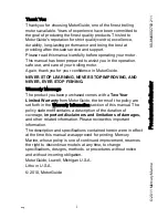
External power connections are made through the +V, -V, VREF 
and Ground connections on the evaluation board. For single 
supply operation, the -V and Ground pins are tied together to the 
power supply negative terminal. For split supplies, +V and -V 
terminals connect to their respective power supply terminals. 
Decoupling capacitors C

2

, C

3

, C

4

 and C

6

 connect to their 

respective supplies through R

11

 and R

14

 resistors. These 

resistors are 100

Ω

 but can be changed by the user to provide 

additional power supply filtering, or to reduce the voltage rate of 
rise to less than ±1V/µs. Two additional capacitors, C5 and C

7

are connected close to the part to filter out high frequency noise. 
Anti-reverse diode D

1

 protects the circuit in the momentary case 

of accidentally reversing the power supplies to the evaluation 
board. The VREF pin can be connected to ground to establish a 
ground referenced input for split supply operation, or can be 
externally set to any reference level for single supply operation.

Amplifier Configuration

A simplified schematic of the evaluation board is shown in 

Figure 2

. The input stage with the components supplied is 

shown in 

Figure 4

with a closed loop gain of 10V/V. The 

differential amplifier gain is expressed in 

Equation 1

:

For single-ended input with an inverting gain G = -10V/V, the 
IN+ input is grounded and the signal is supplied to the IN- 
input. The VREF can be connected to a reference voltage 
between the V+ and V- supply rails. For non-inverting operation 
with G = 11V/V, the IN- input is grounded and the signal is 
supplied to the IN+ input. The non-inverting gain is strongly 
dependent on any resistance from IN- to GND. For good gain 
accuracy, a 0

Ω

 resistor should be installed on the empty R

5


pad. The VREF pin must be connected to ground to establish a 
ground referenced input for dual supply operation, or can be 
externally set to any reference level for single supply 
operation. The VREF should not be left floating.

PCB Layout Considerations

There a few layout constraints to consider when using the 
ISL70219ASEH, but this will generally apply to any generic 
operational amplifier. Analog circuits can conduct noise 
through paths that connect it to the “outside world”. These 
paths include the V+, V-, IN+, IN- and OUT terminals. It’s 
important to make sure these paths are kept away from 
known noise sources to ensure optimal performance of the 
part. If the ISL70219ASEH resides on the same boards as 
digital circuitry it is necessary to decouple the power pins on 
the analog as well as the digital circuitry. This is done on the 
evaluation board with C

2

 through C

7

, with the lower value 

capacitors, C

5

 and C

7

, placed near the V- and V+ pins 

respectively to minimize high frequency noise.

FIGURE 2. BASIC AMPLIFIER CONFIGURATION

IN-

IN+

RF

VREF

IN-

IN+

GND

100k

Ω

RREF+

VOUT

ISL70219 (1/2)

VP

V-

0

Ω

VN

VCM

IN-

IN+

VREF

V+

RIN-

10k

Ω

RIN+

10k

Ω

100k

Ω

RL

DNP

-

+

+

-

-

+

+

-

V

OUT

V

IN+

V

IN-

R

F

R

IN

V

REF

+

=

(EQ. 1)

0.01µF

0.01µF

R14

R1

1

D1

C2

C4

C5

C7

J7

J10

J8

J9

J5

J6

10

0

10

0

1µF

1µF

VREF

V+

V-

FIGURE 3. POWER SUPPLY CIRCUIT

0.1µF

0.1µF

C3

C6

Summary of Contents for ISL70219ASEHEV1Z

Page 1: ... medical and analytical instrumentation precision power supply controls and industrial controls The ordering number for this board is ISL70219ASEHEV1Z Please go to ordering tab on the landing page for the ISL70219ASEH Related Literature ISL70219ASEH Datasheet ISL70219ASEH SMD 5962 14226 ISL70219ASEH Radiation Test Report TR002 Single Event Effects SEE Testing of the ISL70219ASEH Dual Operational A...

Page 2: ...put The VREF can be connected to a reference voltage between the V and V supply rails For non inverting operation with G 11V V the IN input is grounded and the signal is supplied to the IN input The non inverting gain is strongly dependent on any resistance from IN to GND For good gain accuracy a 0Ω resistor should be installed on the empty R5 pad The VREF pin must be connected to ground to establ...

Page 3: ...ables or add a resistor in series with the output FIGURE 4 INPUT STAGE 1 2 FIGURE 5 OUTPUT STAGE 1 2 C1 R 5 R3 J2 J1 R1 R2 R10 R12 R6 R9 R4 DNP DNP DNP OPEN DNP 10k 100k 100k 10k 0 VREF IN IN OUTPUT R26 C6 R 28 DNP OPEN OPEN 0 FROM OUTPUT Bill of Materials DEVICE DESCRIPTION COMMENTS C2 C4 CAP SMD 1206 1µF 50V 10 X7R ROHS Power Supply Decoupling C3 C6 CAP SMD 0805 0 1µF 50V 10 X7R ROHS Power Suppl...

Page 4: ... OUT B OUT A C3 AND C5 CLOSE TO PART V VREF V VREF R8 DNP J10 100K R10 0 01UF C7 JP1 DNP R7 J5 C6 0 1UF R5 DNP LID INB INB INA INA OUTB V V NC OUTA ISL70219ASEHVF U1 1 2 3 4 5 6 7 8 9 10 R2 DNP R20 DNP R11 100 R14 100 R6 10K DNP R23 DNP R1 OPEN C9 J9 R4 10K R24 DNP D1 1 2 3 R22 0 0 01UF C5 OPEN C10 J4 10K R18 J12 C8 OPEN 0 1UF C3 R15 100K J3 J11 R13 100K 0 R21 R12 100K R16 10K J2 R19 0 R9 DNP J7 C...

Page 5: ...UG007 Rev 1 0 Page 5 of 8 Jul 1 2021 ISL70219ASEHEV1Z USER MANUAL ISL70219ASEH Board Layout FIGURE 7 TOP VIEW ...

Page 6: ...00k 1M 10M GAIN dB FREQUENCY Hz ACL1 ACL10 ACL100 ACL1000 60 40 20 0 20 40 60 80 100 1k 10k 100k 1M 10M GAIN dB FREQUENCY Hz ACL1 ACL10 ACL100 ACL1000 10 8 6 4 2 0 2 4 1k 10k 100k 1M 10M FREQUENCY Hz RL 100Ω RL 500Ω RL 5kΩ RL 10kΩ GAIN dB RL 1kΩ 10 8 6 4 2 0 2 4 1k 10k 100k 1M 10M GAIN dB FREQUENCY Hz RL 100Ω RL 500Ω RL 5kΩ RL 10kΩ RL 1kΩ 10 8 6 4 2 0 2 4 6 8 10 1k 10k 100k 1M 10M GAIN dB FREQUENC...

Page 7: ... 2 5V TIME µs SMALL SIGNAL T RANSIENT R ESPONSE mV 10 0 10 20 30 40 50 60 0 5 10 15 20 25 30 35 40 RL 10k AV 1 CL 4pF VOUT 50mVP P VS 5 18V TIME µs LARGE SIGNAL TRANSIENT RESPONSE V 2 4 2 0 1 6 1 2 0 8 0 4 0 0 4 0 8 1 2 1 6 2 0 2 4 0 10 20 30 40 50 60 70 80 90 100 AV 1 CL 4pF VOUT 4VP P VS 5V RL 2k 10k VS 18V RL 2k 10k 0 0 0 1 0 2 0 3 0 4 0 5 0 6 0 7 0 8 75 50 25 0 25 50 75 100 125 150 POSITIVE SL...

Page 8: ...0 04 0 08 0 12 0 16 0 20 0 24 0 10 20 30 40 50 60 70 80 90 TIME µs INPUT VOLTAGE LEVEL V 55 C INPUT 125 C 25 C 0 28 0 24 0 20 0 16 0 12 0 08 0 04 0 0 04 0 10 20 30 40 50 60 70 80 90 TIME µs INPUT VOLTAGE LEVEL V 125 C INPUT 25 C 55 C 0 04 0 0 04 0 08 0 12 0 16 0 20 0 24 0 28 0 10 20 30 40 50 60 70 80 90 TIME µs INPUT VOLTAGE LEVEL V 55 C INPUT 125 C 25 C REVISION DATE DESCRIPTION 1 0 Jul 1 2021 Up...

Page 9: ...RTY RIGHTS These resources are intended for developers skilled in the art designing with Renesas products You are solely responsible for 1 selecting the appropriate products for your application 2 designing validating and testing your application and 3 ensuring your application meets applicable standards and any other safety security or other requirements These resources are subject to change with...

Page 10: ...Mouser Electronics Authorized Distributor Click to View Pricing Inventory Delivery Lifecycle Information Renesas Electronics ISL70219ASEHEV1Z ...

Reviews: