


IRDC3898-P3V3
8/15/2013
Confidential
This evaluation board is a preliminary version meant for the engineering evaluation of the IR3898.
Based on the results of the continuing evaluation, this board can evolve and change without notice
16
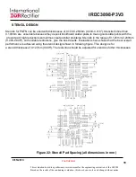
STENCIL DESIGN
Figure 22: Stencil Pad Spacing (all dimensions in mm)
Stencils for PQFN can be used with thicknesses of 0.100-0.250mm (0.004-0.010"). Stencils thinner than
0.100mm are unsuitable because they deposit insufficient solder paste to make good solder joints with the
ground pad; high reductions sometimes create similar problems. Stencils in the range of 0.125mm-0.200mm
(0.005-0.008"), with suitable reductions, give the best results.
Evaluations have shown that the best overall
performance is achieved using the stencil design shown in following figure. This design is for
a stencil thickness of 0.127mm (0.005").The reduction should be adjusted for stencils of other thicknesses.