


IRDC3898-P3V3
8/15/2013
Confidential
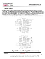
This evaluation board is a preliminary version meant for the engineering evaluation of the IR3898.
Based on the results of the continuing evaluation, this board can evolve and change without notice
15
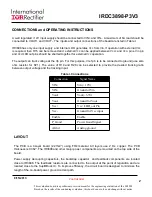
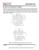
SOLDER RESIST
IR recommends that the larger Power or Land Area pads are Solder Mask Defined (SMD.)
This allows the underlying Copper traces to be as large as possible, which helps in terms of current
carrying capability and device cooling capability. When using SMD pads, the underlying copper
traces should be at least 0.05mm larger (on each edge) than the Solder Mask window,
in order to accommodate any layer to layer misalignment. (i.e. 0.1mm in X & Y.)
However, for the smaller Signal type leads around the edge of the device, IR recommends that
these are Non Solder Mask Defined or Copper Defined. When using NSMD pads,
the Solder Resist Window should be larger than the Copper Pad by at least 0.025mm on
each edge, (i.e. 0.05mm in X&Y,) in order to accommodate any layer to
layer misalignment. Ensure that the solder resist in-between the smaller signal lead areas are at
least 0.15mm wide, due to the high x/y aspect ratio of the solder mask strip.
Figure 21: Solder resist