Intel Quark SE C1000 Platform Manual Download Page 27

 
I2C Interface 


Intel® Quark™ SE Microcontroller C1000 

June 2017 


Platform Design Guide 

Document Number: 334715-004EN 


27 

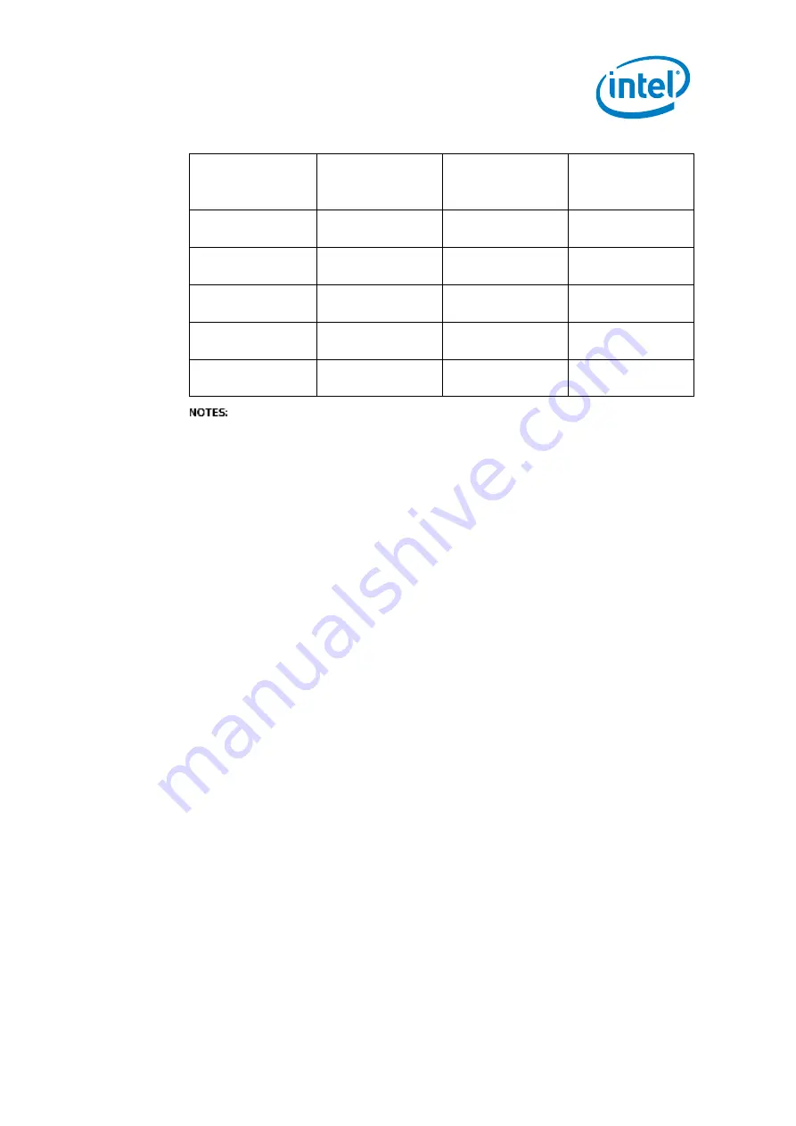
Table 8.  Capacitance Estimates for Calculating Rpu Values 

Capacitance 

Pull-up range  

100 kHz 

Pull-up range  

400 kHz 

Pull-up range 

1000 kHz 

10 pF to 40 pF 

1.1 kΩ to 9.0 kΩ 

2.2 kΩ 

1.0 kΩ to 1.2 kΩ 

40 pF to 100 pF 

1.2 kΩ to 7.2 kΩ 

0.6 kΩ to 2.6 kΩ 

750 Ω 

100 pF to 200 pF 

1.2 kΩ to 4.0 kΩ 

0.6 kΩ to 1.3 kΩ 

500 Ω 

200 pF to 300 pF 

1.2 kΩ to 2.6 kΩ 

0.6 kΩ to 0.9 kΩ 

320 Ω 

300 pF to 400 pF 

1.2 kΩ to 2.0 kΩ 

0.6 kΩ 

240 Ω 


1.


Length matching between Data and Clk is 540 mils. 

2.


Cap per inch of board (pF) = 3 pF/inch (for the current stackup). 

3.


If the nominal trace width is not possible in the breakout area, use 4 mils as the minimum 
trace width. Choose a stackup so that 50 Ohms will be minimum 4 mils. 

4.


It is best to meet nominal impedance and spacing requirement at breakout region. If not, you 
must meet at least the minimum requirement. 

General Design Considerations: 

System designers must consider the total bus capacitance, which includes both SoC 
and device pin capacitance, and board trace length capacitance as well. The number 
and types of I

2

C devices on each I

2

C bus must be determined, not exceeding the 

maximum bus capacitive load of 400 pF for each I

2

C bus. While choosing the pull-

up resistor, it is important to remember that it must not be made so large that the 
bus time constant (Resistance X Capacitance) does not meet the I

2

C rise and fall 

time specification. Analysis of a particular layout is required to confirm correct 
operation. 


§


Summary of Contents for Quark SE C1000

Page 1: ...Document Number 334715 004EN Intel Quark SE Microcontroller C1000 Platform Design Guide June 2017...

Page 2: ...cifications and roadmaps The products described may contain design defects or errors known as errata which may cause the product to deviate from published specifications Current characterized errata a...

Page 3: ...n 13 2 3 Feature Set 14 2 4 Pin Mapping 15 3 0 Subsystem Details 23 3 1 Design Recommendations 23 3 2 General Design Guideline Assumptions 24 4 0 I2 C Interface 25 4 1 I2 C Interfaces Signals 25 4 2 I...

Page 4: ...tion 59 14 2 5 JTAG Pin Termination 59 14 2 6 USB Pin Termination 60 14 2 7 Pin Termination Summary 60 Figures Figure 1 Intel Quark SE Microcontroller C1000 CRB Block Diagram 10 Figure 2 SoC Block Dia...

Page 5: ...n Example 60 Figure 35 USB Pin Termination Example 60 Tables Table 1 Terminology 9 Table 2 Reference Documents 9 Table 3 Stackup Details 13 Table 4 Alphabetical Ball Listing for BGA package 16 Table 5...

Page 6: ...6 Document Number 334715 004EN Table 25 Generic Routing Requirements 44 Table 26 ADC Signals 46 Table 27 USB Signals 48 Table 28 USB Routing Requirements 49 Table 29 Timing Parameters for External Reg...

Page 7: ...une 2017 004 Corrections in Table 14 SPI Signals Added Chapter 14 0 describing optimal termination of unused pins February 2017 003 Corrections in external power supply section Added reference to HOST...

Page 8: ...00 processor based platform This work is ongoing and these recommendations are subject to change Caution If the guidelines listed in this document are not followed it is very important that the design...

Page 9: ...ose Input Output I2 C Inter Integrated Circuit I2S Inter IC Sound JTAG Joint Test Action Group OSC Oscillator PWM Pulse Width Modulation RTC Real Time Clock SIO Serial I O SoC System on Chip SPI Seria...

Page 10: ...ns This section covers general assumptions about the Intel Quark SE SoC microcontroller and Intel Quark SE microcontroller C1000 Customer Reference Board CRB system topology and interface connectivity...

Page 11: ...tackup of a motherboard such as changes in the dielectric height trace widths and spacing can impact the impedance or loss and jitter characteristics of all interfaces Such changes may be intentional...

Page 12: ...s must be used in conjunction with high speed signal layer transitions that include a reference plane change Refer to each signal group section for more specification The parameter values for internal...

Page 13: ...oefficient to choose proper trace spacing The coupling coefficient represents the source voltage percentage that is coupled to victim lines As shown in Figure 5 Kb is defined as the backward coupling...

Page 14: ...3 2 3 Feature Set A device can contain any feature set and capabilities supported on the Intel Quark SE microcontroller C1000 The following is a feature set of a sample wearable device used in the Int...

Page 15: ...ino Uno like SIL sockets 1 8V and 3 3V IO Intel Quark SE microcontroller C1000 on board components Accelerometer Gyroscope and Temperature sensors UART JTAG to USB convert for USB debug port Other Int...

Page 16: ...Listing for BGA package Ball Assign Function_0 Function_1 Function_2 Description A1 VSS Ground A2 GPIO 27 SPI0_M_CS_B 3 GPIO 27 SPI0 Master Chip Select 3 A3 GPIO 21 SPI0_M_SCK GPIO 21 SPI0 Master Cloc...

Page 17: ...22 I2S transmit data B4 GPIO 16 I2S_RSCK GPIO 16 I2S Receive Clock B5 GPIO 12 SPI1_M_CS_B 1 GPIO 12 SPI1 Master Chip Select 1 B6 GPIO 9 SPI1_M_MISO GPIO 9 SPI1 Master Master In Slave Out B7 SPI1_SS_MO...

Page 18: ...ter Master Out Slave In D4 GPIO 17 I2S_RWS GPIO 17 I2S Receive Write Select D5 GPIO 14 SPI1_M_CS_B 3 GPIO 14 SPI1 Master Chip Select 3 D6 GPIO 8 SPI1_M_SCK GPIO 8 SPI1 Master Serial Clock D7 SPI1_SS_C...

Page 19: ...GPIO 3 Analog Input 3 SPI slave Master Out Slave in F1 GPIO_AON 4 Always On GPIO 4 F2 GPIO_AON 3 Always On GPIO 3 F3 GPIO_AON 0 Always On GPIO 0 F4 GPIO_AON 2 Always On GPIO 2 F5 GPIO_AON 1 Always On...

Page 20: ...H4 VCC_AON_1P8 1 8v supply voltage for Always On counter H5 VCC_AON_1P8 1 8v supply voltage for Always On counter H6 VSS_GNDSENSE_ESR1 Ground for switching regulator 1 H7 VCC_PLL_1P8 1 8 PLL supply v...

Page 21: ...2 K3 PLT_REG_EN K4 VCCOUT_QLR2_1P8 Output voltage for linear reg2 K5 VCCOUT_QLR1_3P3 Output voltage for linear reg1 K6 VCCOUT_HOST_1P8 1 8 host supply output K7 VCC_HOST_1P8 K8 GPIO 7 AIN 7 GPIO 7 Ana...

Page 22: ...12 VCC_USB_3P3 3 3 supply voltage for USB M1 VSS Ground M2 VCC_BATT_ESR1_3P7 Mains supply voltage for ESR1 M3 VCCOUT_AON_1P8 1 8 Always On Supply voltage M4 VCCOUT_PLAT_1P8_1P8 Output voltage for swit...

Page 23: ...orage and I O interfaces into a single system on chip solution This section presents design recommendations for the subsystems that make up the Intel Quark SE microcontroller C1000 platform It include...

Page 24: ...ion Note All routing guidelines in this document are simulated based on the CRB stackup Note For technical specifications such as speeds supported resolutions and data rates please refer to the Intel...

Page 25: ...n Type Description I2C_M_x_CLK I O I2 C Serial Clock I2C_M_x_DATA I O I2 C Serial Data The following is a list of the I2 C features Two I2 C interfaces Support for both master and slave operation Oper...

Page 26: ...I2 C I2 C SDA SCL Breakout Segment trace Transmission Line Segment Breakoutsoc L1 L4 Routing Layer Microstrip Stripline MS SL MS SL Characteristic Impedance 50 10 MS 50 10 SL 50 10 MS 50 10 SL Trace...

Page 27: ...the breakout area use 4 mils as the minimum trace width Choose a stackup so that 50 Ohms will be minimum 4 mils 4 It is best to meet nominal impedance and spacing requirement at breakout region If no...

Page 28: ...ing is a list of PWM features Four counters capable of operating in PWM Mode or Timer Mode PWM Mode Configurable high and low times for each PWM Output Minimum high and low time of 2 32MHz clock perio...

Page 29: ...figured as follows This assumes a nominal system clock frequency of 32 MHz The values in nanoseconds will differ if the system clock frequency is changed Table 10 PWM Timing Characteristic Value Syste...

Page 30: ...5 004EN Table 11 Timer Period Characteristic Value System Clock Cycles Value Time Timeout Period Granularity 1 31 25 ns Timeout Period Range 0 to 4294967295 2 32 1 0 to 134 22 s Timer Mode supports th...

Page 31: ...lds Supports 8 bit operation mode Supports RS485 and RS232 Supports DTR DCD DSR RI Modem Control Pins through GPIO pins controlled by software 6 1 Signal Descriptions Table 12 UART Signals Signal Name...

Page 32: ...y The following is a list of the UART controller features Operation compliant with the 16550 Standard Start bit 5 to 8 bits of data Optional Parity bit Odd or Even 1 1 5 or 2 Stop bits Baud rate confi...

Page 33: ...ign Guide Document Number 334715 004EN 33 Fractional clock divider that ensures less than 2 frequency error for most supported baud rates Fraction resolution is 4 bits Exception 2 07 error for 1 391 M...

Page 34: ...PI Master Output Slave Input SPI_M_x_MISO Input SPI Master Input Slave Output The Intel Quark SE microcontroller C1000 includes the following Two SPI master interfaces with support for SPI clock frequ...

Page 35: ...e Spacing S2 Between SPI signals and other signals 5 mils 3W 2W Trace Spacing S3 Between SPI_CLK to other signals 5 mils 3W 2W Trace Length 100 mils 1500 mils TL0 TL1 TL2 10000 mils 500 mils Length mi...

Page 36: ...edance Trace Spacing S1 Between SPI signals 4 mils 3W 3W 2W Trace Spacing S2 Between SPI signals and other signals 5 mils 3W 3W 2W Trace Spacing S3 Between SPI_CLK to other signals 5 mils 3W 3W 2W Tra...

Page 37: ...other signals 5 mils 3W 2W Trace Spacing S3 Between SPI_CLK to other signals 5 mils 3W 2W Trace Length 100 mils 1500 mils TL0 TL1 TL2 8000 mil 500 mils Length mismatch between SPI_CLK and SPI_CS 250...

Page 38: ...Interrupt Control FIFO mode support with 16B deep TX and RX FIFOs The following is a list of the SPI slave features One SPI slave interface Frame formats Motorola SPI Texas Instruments SSP National S...

Page 39: ...ection Type Description HYB_XTALI I O XTAL Input or External System Clock HYB_XTALO I O XTAL Input RTC_XTALI I O RTC XTAL Input RTC_XTALO I O RTC XTAL Input RTC_CLK Output RTC Clock Output SYS_CLK Out...

Page 40: ...10 Trace Width w Meet impedance Meet impedance Trace Spacing S to other signals 15 mils 25 mils Trace Length 250 mils Total Trace Length Total Length 1000 mils Number of vias allowed 2 Via stub lengt...

Page 41: ...2 pF CL Crystal Load Cap 7 pF Ftol Frequency Tolerance 20 20 ppm Dlev Drive Level 1 uW 8 2 Features The following is a list of the RTC features Programmable 32 bit binary counter Counter increments o...

Page 42: ...bling proper configuration The SoC contains two instances of the GPIO controller The GPIO controller provides a total of 32 independently configurable GPIOs All GPIOs are interrupt capable supporting...

Page 43: ...Spacing S2 Between SPI signals and other signals 5 mils minimum 3W 5 mils minimum Trace Length 0 5 max 9 max 0 5 max Trace Total Length Total trace length 10 max 1 Rs 22 or 33 ideally closer to driver...

Page 44: ...uting Termination Route for TDO Termination Route for TDI TMS TCK Transmission Line Segment TL1 TLterm2 TLterm1 Routing Layer Microstrip Stripline Dual Stripline MS SL MS SL MS SL Characteristic Imped...

Page 45: ...C1000 June 2017 Platform Design Guide Document Number 334715 004EN 45 10 2 Features The following is a list of the JTAG Interface features 5 pin IEEE 1149 1 JTAG Interface Boundary scan support ARC me...

Page 46: ...scriptions Figure 21 Analog Shielding Requirement The previous figure shows an example analog signal traces A B and C are shielded agnd net with metal layers traces adjacent above and below the signal...

Page 47: ...ontroller C1000 June 2017 Platform Design Guide Document Number 334715 004EN 47 Latencies Power up time of 10 us 1 conversion cycle resolution bits 2 cycles Full scale input range is 0 to AVDD ADC Ref...

Page 48: ...ents a single USB 1 1 device controller Table 27 USB Signals Signal Name Direction Type Description USB_PADP I O USB Positive differential signal USB_PADN I O USB Negative differential signal USB_VDD3...

Page 49: ...4H max 25 mils or 5H max 25 mils or 5H Trace Spacing S3 Between diff pairs and high speed CLK signals 4H 50 mils 50 mils Trace Length 200 mils TL0 TL1 TL2 TL3 7500 mils TL2 TL3 500 mils Length mismat...

Page 50: ...ts control interrupt and bulk transfers does not support isochronous transfers Supports a maximum packet size of 64 bytes Supports dedicated FIFOs per IN endpoint Each Transmit FIFO is sized at two ma...

Page 51: ...he SoC when an external platform power source is required 1 Tie the strap pin PLT_REG_EN to the VCC_AVD_OPM_2P6 power rail This voltage is an output from the SoC VCCOUT_AVD_OPM_2P6 Caution Special car...

Page 52: ...EF_EN VCC_SENSE_ESR1 VCCOUT_QLR1_3P3 VCCOUT_ESR1_3P3 VSS_GNDSENSE_ESR1 VCC_SENSE_ESR3 VCCOUT_QLR3_1P8 VCCOUT_ESR3_1P8 VSS_GNDSENSE_ESR3 VCC_AVD_OPM_2P6 VCC_IO_AON VCC_AON_1P8 1 8V from external supply...

Page 53: ...The following guidelines describe how to terminate the unused internal VR signals in this implementation 1 Tie PWR_REG_EN signal to reference plane GND 2 Connect the following unused internal VR sign...

Page 54: ...levels in VCC_AVD_OPM_2P6 at any time refer to the Intel Quark SE Microcontroller C1000 Power Sequencing Considerations Application Note 7 Disable the unused internal VR by software during the initia...

Page 55: ...Power Intel Quark SE Microcontroller C1000 June 2017 Platform Design Guide Document Number 334715 004EN 55 Figure 28 Power Sequence for Internal Regulator...

Page 56: ...be initiated as inputs or in high resistance states to avoid shorted outputs implications Pulling down to VSS consumes about 15 less power than pulling up to VCC for CMOS technology based components T...

Page 57: ...GPIO Pin Termination Example External Pull Down Resistor GPIO_9_SPI1_M_MISO B6 10 k RPD Intel Quark SE Microcontroller C1000 BGA 144 Package 14 2 2 Sensor Subsystem SPI Pin Termination Unused Sensor...

Page 58: ...connected to VSS through for example 10 k pull down resistors Figure 31 illustrates termination of the I2C0_SDA pin ball B12 This analogy should apply to terminating any other I2 C pins including the...

Page 59: ...d by connecting them to VCC through pull up for example 10 k resistors Figure 33 illustrates this termination Figure 33 UART Pin Termination Example UART0_RXD_AIN_18 E8 Intel Quark SE Microcontroller...

Page 60: ...BGA 144 Package 14 2 6 USB Pin Termination When the USB module will not be used the differential pair on unused downstream ports should be tied together and pulled down to ground through for example...

Page 61: ...or 1 10 k RPU to VCC A12 VSS Ground N A B1 GPIO_SS 11 GPIO Sensor Subsystem 11 1 10 k RPD to VSS B2 GPIO 26 GPIO 26 1 10 k RPD to VSS B3 GPIO 20 GPIO 22 1 10 k RPD to VSS B4 GPIO 16 GPIO 16 1 10 k RPD...

Page 62: ...S_B 3 SPI1 Sensor Subsystem Chip Select 3 1 10 k RPD to VSS D8 SPI1_SS_CS_B 2 SPI1 Chip Select 2 on Sensor Subsystem 1 10 k RPD to VSS D9 SPI0_SS_CS_B 1 SPI0 Sensor Subsystem Chip Select 1 1 10 k RPD...

Page 63: ...G8 VCC_IO_AON Input voltage for Always On I O N A G9 GPIO_SS 2 GPIO for Sensor Subsystem 2 1 10 k RPD to VSS G10 GPIO_SS 3 GPIO for Sensor Subsystem 3 1 10 k RPD to VSS G11 GPIO_SS 4 GPIO for Sensor...

Page 64: ...OST_1P8 1 8 host supply output N A K7 VCC_HOST_1P8 N A K8 GPIO 7 GPIO 7 1 10 k RPD to VSS K9 GPIO_SS 7 GPIO for Sensor Subsystem 7 1 10 k RPD to VSS K10 GPIO_SS 6 GPIO for Sensor Subsystem 6 1 10 k RP...

Page 65: ...LAT_1P8_1P8 Output voltage for switching reg2 N A M5 VCCOUT_PLAT_3P3_3P3 Output voltage for switching reg1 N A M6 VCCOUT_HOST_1P8_1P8 1 8 Supply voltage for switching reg3 N A M7 VSS_GNDSENSE_ESR3 Gro...

Reviews: