


GUIDELINE: Register interface I/O at the FPGA I/O boundary.
With core and I/O delays easily exceeding 8 ns, it is recommended to register these
buses in each direction in I/O Element (IOE) registers, so they remain aligned as they
travel across the core FPGA logic fabric. On the transmit data and control, maintain
the clock-to-data/control relationship by latching these signals on the falling edge of
the
emac[0,1,2]_gtx_clk
output from the HPS EMAC. Latch the receive data and
control at the FPGA I/O inputs on the rising edge of the
RX_CLK
sourced by the PHY.
GUIDELINE: Consider transmit timing in MII mode.
MII is 25 MHz when the PHY is in 100 Mbps mode and 2.5 MHz when the PHY is in 10
Mbps mode, so the shortest period is 40 ns. The PHY sources the clock for both
transmit and receive directions. Because the transmit timing is relative to the
TX_CLK
clock provided by the PHY, the turnaround time may be of concern, but this is usually
not an issue due to the long 40-ns period.
Note:
The transaction is routed through the FPGA, then out for the data. The round-trip
delay must be less than 25 ns, because there is a 15-ns input setup time. The
transmit data and control are launched into the FPGA fabric by the HPS EMAC transmit
path logic on the negative edge of the PHY-sourced
TX_CLK
, which removes 20 ns of
the 40-ns clock-to-setup timing budget.
With the round trip clock path delay on the data arrival timing incurring PHY-to-SoC
board propagation delay plus the internal path delay from the SoC pin to and through
the HPS EMAC transmit clock mux taking away from the remaining 20-ns setup timing
budget, it may be necessary to retime the transmit data and control to the rising edge
of the
phy_txclk_o
clock output registers in the FPGA fabric for MII mode transmit
data and control.
4.5.1.2.2. Adapting to RGMII
It is possible to adapt the GMII HPS EMAC PHY signals to an RGMII PHY interface at
the FPGA I/O pins using logic in the FPGA. While it is possible to design custom logic
for this adaptation, this section describes using Platform Designer (Standard) adapter
IP.
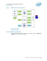
GUIDELINE: Use the GMII-to-RGMII Adapter IP available in Platform
Designer (Standard).
Configure the HPS component in Platform Designer (Standard) for an EMAC as “FPGA”
I/O instance. Do not export the resulting HPS component GMII signals in Platform
Designer (Standard). Instead, add the Intel HPS GMII to RGMII Converter to the
Platform Designer (Standard) subsystem and connect to the HPS component’s GMII
signals. The GMII to RGMII Converter uses the Intel HPS EMAC Interface Splitter in
Platform Designer (Standard) to split out the
emac
conduit from the HPS component
for use by the GMII to RGMII Converter. See the
Embedded Peripherals IP User Guide
for information on how to use the Intel HPS GMII to RGMII Converter.
GUIDELINE: Provide a glitch-free clock source for the 10/100 Mbps modes.
In an RGMII PHY interface, the
TX_CLK
is always sourced by the MAC, but the HPS
component’s GMII interface expects
TX_CLK
to be provided by the PHY device in
10/100 Mbps modes. The GMII to RGMII adaptation logic must provide the 2.5/25
MHz
TX_CLK
on the GMII’s
emac[0,1]_tx_clk_in
input port, and the switch
between 2.5 MHz and 25 MHz must be accomplished in a glitch-free manner as
4. Board Design Guidelines for SoC FPGAs
AN-796 | 2018.06.18
AN 796: Cyclone V and Arria V SoC Device Design Guidelines
40