background image

CY8CKIT-064S0S2-4343W PSoC 64 Standard Secure – AWS Wi-Fi BT Pioneer Kit Guide, Doc. # 002-30680 Rev. *B

43

Hardware

4.2.9

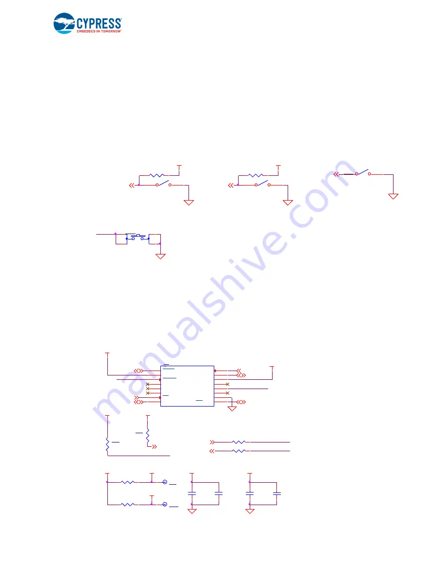
Push Buttons

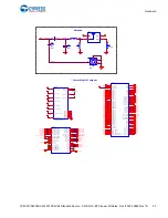
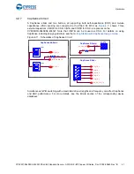
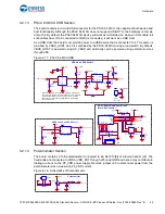
The board has a reset button, two user-controllable buttons and a KitProg3 Mode selection button. 
The reset button (

SW1

) is connected to the XRES pin of the PSoC 64 MCU and is used to reset the 

device. Two  user  buttons  (

SW2

  and 

SW4

)  are  connected  to  pin  P0[4]  and  P1[4]  of  the  PSoC  64 

MCU  respectively.  In  addition,  the  Mode  selection  button  (

SW3

)  is  connected  to  the  PSoC  5LP


device for programming mode selection (Refer to the 

KitProg3 User Guide

 for details). All buttons 

are active LOW configuration and short to GND when pressed. The CY8CMOD-064S0S2-4343W


has a pull-up on the PSoC 64 MCU XRES line.

Figure 4-13.  Schematics of Push Buttons

4.2.10

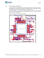
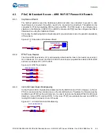
Cypress Quad SPI NOR Flash

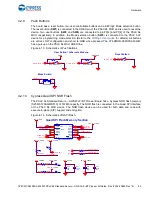
The PSoC 64 Standard Secure – AWS Wi-Fi BT Pioneer Board has a Cypress NOR flash memory 
(S25FL512SAGMFI010) of 512Mb capacity. The NOR flash is connected to the Quad SPI interface 
of  the  PSoC  64  MCU  device.  The  NOR  flash  device  can  be  used  for  both  data  and  code  with 
execute-in-place (XIP) support and encryption.

Figure 4-14.  Schematics of QSPI Flash


SW4
EVQ-PNF04M

SW2
EVQ-PNF04M

USER_BTN_1

R20

10K

User Button / Hibernate Wakeup

VBACKUP

USER_BTN_2

VDDD

R110

10K


SW1
EVQ-PE105K

Reset Button

XRES_L_MCU


SW3

SKRPACE011

1

4

2

3

P5LP1_2

Mode Switch


R90

0 OHM

C54
0.1uF
16V

C32
0.1uF
16V

C56
1uF
10V

R26

0 OHM

C55
1uF
10V

VCC_IO_FLASH

VCC_FLASH

VCC_IO_FLASH

VCC_FLASH

VCC_VDDIO0

Quad SPI Flash Memory Section

R107

0 OHM

No Load

IO6

FLASH_RST_L

FLASH_SS_L

TP9

TP20

U3

S25FL512SAGMFI010

HOLD /IO3

1

VCC

2

RESET /RFU

3

DNU_1

4

DNU_2

5

DNU_3

6

CS

7

SO/IO1

8

WP /IO2

9

VSS

10

DNU_4

11

DNU_5

12

DNU_6

13

DNU_7

14

SI /IO0

15

SCK

16

FLASH_INT_L

FLASH_SS_L

IO5

QSPI_IO1

QSPI_IO0

QSPI_SCK

QSPI_IO3

QSPI_IO2

R138

0 OHM

No Load

FLASH_INT_L

FLASH_INT_L

FLASH_RST_L

R93

10K

VCC_IO_FLASH

R92
10K

No Load

VCC_IO_FLASH

VCC_FLASH

VCC_IO_FLASH

Summary of Contents for Cypress CY8CKIT-064S0S2-4343W

Page 1: ...ers as part of the Infineon product portfolio Continuity of document content The fact that Infineon offers the following product as part of the Infineon product portfolio does not lead to any changes to this document Future revisions will occur when appropriate and any changes will be set out on the document history page Continuity of ordering part numbers Infineon continues to support existing pa...

Page 2: ...CY8CKIT 064S0S2 4343W PSoC 64 Standard Secure AWS Wi Fi BT Pioneer Kit Guide Doc 002 30680 Rev B Cypress Semiconductor 198 Champion Court San Jose CA 95134 1709 www cypress com ...

Page 3: ... you shall and hereby do release Cypress from any claim damage or other liability arising from any Security Breach In addition the products described in these materials may contain design defects or errors known as errata which may cause the product to deviate from published specifications To the extent permitted by applicable law Cypress reserves the right to make changes to this document without...

Page 4: ...6 3 Provisioning Overview for PSoC 64 Standard Secure AWS MCU s 27 3 1 Provisioning Overview 27 4 Hardware 29 4 1 Schematics 29 4 2 Hardware Functional Description 29 4 2 1 CY8CMOD 064S0S2 4343W MOD1 29 4 2 2 PSoC 5LP based KitProg3 U2 34 4 2 3 Serial Interconnection between PSoC 5LP and PSoC 64 MCU 35 4 2 4 Serial Interconnection between PSoC 5LP and CYW4343W 36 4 2 5 Power Supply System 36 4 2 6...

Page 5: ...2 30680 Rev B 4 Contents 4 3 3 microSD Card Detect Multiplexing 46 4 3 4 microSD Card SPI Multiplexing 47 4 3 5 U FL UMCC Connector for External Antenna 47 4 3 6 U FL UMCC Connector for Antenna Diversity 47 4 4 Bill of Materials 48 4 5 Frequently Asked Questions 48 Revision History 50 ...

Page 6: ... to obtain a new FCC ID for this host kit Most conducted RF test results may still be reused Customer also needs to take their product through other FCC ISED testing such as unintentional radiators FCC sub part 15B and any other required regional product certifications including but not limited to EU directives Refer FCC Regulatory Certification Guide by Murata on information on pre certified and ...

Page 7: ...cedures only at an ESD workstation If an ESD workstation is unavailable use appropriate ESD protection by wearing an anti static wrist strap attached to a grounded metal object Handling Boards CY8CKIT 064S0S2 4343W PSoC 64 Standard Secure AWS Wi Fi BT Pioneer Kit is sensitive to ESD Hold the board only by its edges After removing the board from its box place it on a grounded static free surface Us...

Page 8: ...RTOS support that communicates with the secure execution environment The PSoC 64 Standard Secure AWS Wi Fi BT Pioneer Board offers compatibility with Arduino shields The board features a PSoC 64 MCU and a CYW4343W Wi Fi Bluetooth combo module Cypress CYW4343W is a highly integrated single chip solution that includes a 2 4 GHz WLAN IEEE 802 11 b g n MAC baseband radio and Bluetooth 5 1 support The ...

Page 9: ...as the following contents as shown in Figure 1 1 PSoC 64 Standard Secure AWS Wi Fi BT Pioneer Board USB Type A to Micro B cable Four jumper wires 4 inches each Two jumper wires 5 inches each Quick Start Guide Promotional Code for 10 in AWS Credits Figure 1 1 Kit Contents Inspect the contents of the kit if you find any part missing contact your nearest Cypress sales office for help www cypress com ...

Page 10: ...s a detailed hardware description methods to use the onboard NOR flash kit schematics and the bill of materials BOM 1 3 Code Examples A list of supported code examples can be found in the Build and Run section of the getting started document under Running other demos 1 4 Board Details The PSoC 64 Standard Secure AWS Wi Fi BT Pioneer Board has the following features CY8CMOD 064S0S2 4343W carrier mo...

Page 11: ... button with Hibernate wakeup capability GPIO on non Arduino header J21 9 P0 5 RGB green LED LED5 GPIO on non Arduino header J24 3 BT_UART_RXD BT_UART_TXD BT_UART_CTS BT_UART_RTS NC NC WL_GPIO_4 NC BT_I2S_CLK BT_I2S_WS BT_I2S_DO BT_I2S_DI NC BT_IO3 BT_IO4 BT_IO5 Arduino Uno R3 LEGEND PSoC 6 I Os WL BT I Os NC VTRAG IOREF XRES RESET V 3 3 3 3V V 5 0 5V GND GND GND GND VIN Vin P6_0 SCL P6_1 SDA VREF...

Page 12: ...Arduino header P5 1 UART_TX Arduino D1 J4 2 Remove R61 to disconnect from KitProg3 Populate R116 to connect to GPIO on non Arduino header P5 2 UART_RTS Arduino D2 J4 3 Remove R19 to disconnect from KitProg3 P5 3 UART_CTS Arduino D3 J4 4 Remove R18 to disconnect from KitProg3 P5 4 Arduino D4 J4 5 P5 5 Arduino D5 J4 6 P5 6 Arduino D6 J4 7 P5 7 Arduino D7 J4 8 P6 0 I2C SCL Arduino J3 10 Remove R58 to...

Page 13: ...eader IO11 J21 4 Remove R29 to disconnect from CapSense Populate R152 to connect to GPIO on non Arduino header P8 5 CapSense Slider2 RX GPIO on non Arduino header IO12 J21 5 Remove R30 to disconnect from CapSense Populate R153 to connect to GPIO on non Arduino header P8 6 CapSense Slider3 RX GPIO on non Arduino header IO13 J21 6 Remove R31 to disconnect from CapSense Populate R151 to connect to GP...

Page 14: ... output Extended Arduino A6 J2 13 Remove R51 to disconnect from potentiometer P10 7 Extended Arduino A7 J2 15 P11 0 QSPI F RAM CS P11 1 Red user LED LED9 GPIO on non Arduino header J24 4 P11 2 QSPI Flash CS P11 3 6 QSPI Flash IO 3 0 P11 7 QSPI Flash CLK P12 0 Arduino header D11 J3 4 P12 1 Arduino header D12 J3 5 P12 2 Arduino header D13 J3 6 P12 3 Arduino header D10 J3 3 P12 4 microSD card CMD Rem...

Page 15: ...L P13 4 GPIO on non Arduino header IO5 J22 6 P13 5 GPIO on non Arduino header IO6 J22 7 P13 6 GPIO on non Arduino header IO3 J22 4 P13 7 microSD card chip detect GPIO on non Arduino header IO16 J24 6 Remove R161 to disconnect from microSD card detect Populate R160 to connect to IO16 J24 6 CYW4343W Pins BT_UART_TXD UART interface with Host MCU PSoC 64 MCU BT_UART_RXD UART interface with Host MCU PS...

Page 16: ...nts Local Sales Office Locations 1 7 Documentation Conventions BT_IO_3 Bluetooth general purpose I O BT_IO_4 Bluetooth general purpose I O BT_IO_5 Bluetooth general purpose I O WL_GPIO_4 Programable GPIO Table 1 2 Document Conventions for Guides Convention Usage Courier New Displays file locations user entered text and source code C cd icc Italics Displays file names and reference documentation Re...

Page 17: ...External Crystal Oscillator ESD Electrostatic Discharge ETM Embedded Trace Macrocell GPIO General Purpose Input Output HID Human Interface Device I2C Inter Integrated Circuit I2S Inter IC Sound IC Integrated Circuit IDE Integrated Development Environment IoT Internet of Things LED Light emitting Diode LPO Low Power Oscillator PC Personal Computer PDM Pulse Density Modulation PSoC Programmable Syst...

Page 18: ...Fi BT Pioneer Kit Guide Doc 002 30680 Rev B 17 Introduction SWD Serial Wire Debug UART Universal Asynchronous Receiver Transmitter USB Universal Serial Bus WCO Watch Crystal Oscillator Table 1 3 Acronyms Used in this Document continued Acronym Definition ...

Page 19: ...TF Encryption Decryption USB FS eFuse 1024 bits Profiler LCD Audio Subsystem PDM PCM 2x I2S SCB I2C or SPI 32x TCPWM CapSense LP Comparator Programmable Analog SAR ADC 12 bit SARMUX Temperature Sensor I O Subsystem Up to 102 GPIOs including 6 OVT 128 TQFP Package Boundary Scan 2x Smart I O Ports USB PHY System Interconnect Multi Layer AHB IPC MPU SMPU Cortex M4F CPU 150 50 MHz 1 1 0 9 V SWJ ETM IT...

Page 20: ...4 I Os Control 5 I Os 77 I Os USB XRES 25 I Os 3 3V 1 8 3 3V 3 6V 1 8 3 3V 3 2 4 2V Chip Antenna USB Micro B KitProg3 PSoC 5LP KitProg3 Mode Switch LED Carrier Module 10 pin SWD JTAG Header 20 pin ETM Header Reset Button microSD Card Slot PSoC 64 MCU I O Headers Arduino User LEDs RGB Red Orange I2C UART_RX UART_TX SWD SWD JTAG TRACE QSPI NOR Flash SWD JTAG P5LP_VDD VTARG VDDIO0 2 x User Buttons 2 ...

Page 21: ...dard Secure AWS Wi Fi BT Pioneer Kit comes with the PSoC 64 Standard Secure AWS Wi Fi BT Pioneer Board Figure 2 4 and Figure 2 5 show the markup of the Pioneer Board Figure 2 4 PSoC 64 Standard Secure AWS Wi Fi BT Pioneer Board Top View 1 2 3 4 5 6 7 8 9 11 10 10 12 13 14 15 16 17 18 21 20 19 23 22 24 25 26 27 28 29 30 31 29 32 33 34 17 30 30 17 35 36 ...

Page 22: ...h is required to blow eFuses 4 KitProg3 programming mode selection button SW3 This button can be used to switch between various modes of operation of KitProg3 CMSIS DAP BULK CMSIS DAP HID or DAPLink modes For more details see the KitProg3 User Guide 5 PSoC 64 MCU VDD current measurement jumper J15 An ammeter can be connected to this jumper to measure the current consumed by the PSoC 64 MCU VDD pow...

Page 23: ... default For detailed information on how to rework the kit to access these pins see Table 1 1 on page 10 18 CapSense slider SLIDER and buttons BTN0 and BTN1 The CapSense touch sensing slider and two buttons all of which are capable of both self capacitance CSD and mutual capacitance CSX operation allow you to evaluate Cypress fourth generation CapSense tech nology The slider and buttons have a 1 m...

Page 24: ...on board peripherals see Table 1 1 on page 10 for pin mapping These are not loaded by default 31 RGB LED LED5 This onboard RGB LED can be controlled by the PSoC 64 MCU The LEDs are active LOW so the pins must be driven to ground to turn ON the LEDs 32 Wi Fi BT GPIO header J23 This header brings out a few I Os of the CYW4343W for general purpose applications This is not loaded by default 33 PSoC 64...

Page 25: ...de for programming and debugging For detailed instructions see Help ModusToolbox IDE Documentation User Guide Connect the board to the PC using the USB cable as shown in Figure 2 6 It enumerates as a USB Composite Device if you are connecting it to your PC for the first time KitProg3 operates in either CMSIS DAP Bulk mode or DAPLink mode default DAPLink mode is required for provisioning the PSoC 6...

Page 26: ...board as Figure 2 7 shows Figure 2 7 UART Connection between KitProg3 and PSoC 64 MCU The secondary UART and flow control lines between the CYW4343W and the KitProg3 are hard wired on the board as Figure 2 8 shows Figure 2 8 UART Connection between KitProg3 and CYW4343W For more details on the KitProg3 USB UART functionality see the KitProg3 User Guide LW3URJ 36R 0 8 Wͺh ZdϭͺZy Wͺh Zdϭͺ d Wͺh Zdϭͺ...

Page 27: ... as an I2C master The I2C lines on the PSoC 64 MCU are hard wired on the board to the I2C lines of the KitProg3 with onboard pull up resistors as Figure 2 9 shows The USB I2C supports I2C speeds of 50 kHz 100 kHz 400 kHz and 1 MHz For more details on the KitProg3 USB I2C functionality see the KitProg3 User Guide Figure 2 9 I2C Connection between KitProg3 and PSoC 64 MCU KitProg3 PSoC 64 MCU P6 1 P...

Page 28: ...s by which secure assets like keys and security policies are injected into the device This step typically occurs in a secure manufacturing environment that has a Hardware Security Module HSM For a more detailed overview of what provisioning entails see Chapter 2 of the Secure Boot SDK User Guide In the context of evaluating this kit the provisioning flow can be visualized as follows Figure 3 1 Pro...

Page 29: ...hip has been provisioned with the Public Image key it will only boot images signed by the associated Private key Optionally the image can be encrypted if the Boot and Upgrade policy specifies it The signing and encryption process is a post build script provided by the Secure Boot SDK The build and encrypt signing flow for a CY8CKIT 064S0S2 4343W target using the ModusToolbox make process is shown ...

Page 30: ... pre certified Type 1DX module with CYW4343W from Murata LBEE5KL1DX is used for ease of development CYW4343W supports only the 2 45 GHz band but the antenna used is a 2450AD14A5500 Dual Band 2 45 GHz 5 5 GHz Mini Chip Antenna from Johanson to use the same antenna across different designs The castellated PCB module has 137 castellated pads which are used for different voltage rails and I O signals ...

Page 31: ...5_7 SDIO_DATA1 P12_3 BT_DEV_WAKE P11_4 P12_6 P0_4 P8_3 P9_0 BT_UART_RTS R6 47K P10_5 P13_4 P6_7 R4 47K DNI P1_5 P7_6 P9_1 P9_6 U1A CYS0644ABZI S2D44 P0 0 E3 P0 1 E2 P0 2 E1 P0 3 F3 P0 4 F2 P0 5 G3 P1 0 G2 P1 1 G1 P1 2 H3 P1 3 H2 P1 4 H1 P1 5 J3 P5 0 N7 P5 1 L8 P5 2 M8 P5 3 N8 P5 4 L9 P5 5 M9 P5 6 N9 P5 7 N10 P6 0 M10 P6 1 L10 P6 2 L11 P6 3 M11 P6 4 N11 P6 5 M12 P6 6 N12 P6 7 M13 P7 0 L13 P7 1 L12 ...

Page 32: ... 1 3 2 4 P12_7 P12_6 C22 10pF 25V C26 10pF 25V ECO VDDIO_WL VBAT LBEE5KL1DX 883 U2A VBAT 30 VIO 36 SR_VLX 34 VIN_LDO 31 GND1 1 GND2 12 GND3 19 GND4 21 GND5 29 GND6 35 GND7 40 GND8 42 GND9 43 GND10 44 GND11 45 GND12 46 GND_SR_PVSS1 32 GND_SR_PVSS2 33 L3 2 2uH C29 4 7uF 16V Supply for Type 1DX Module CY8CKIT 064S0S2 4343W PSoC 64 Standard Secure AWS Wi Fi BT Pioneer Kit Guide Doc 002 30680 Rev B 31 ...

Page 33: ...dule Signals LBEE5KL1DX 883 U2B WL_REG_ON 28 WL_HOST_WAKE 27 SDIO_CLK 20 SDIO_CMD 22 SDIO_DATA_0 24 SDIO_DATA_1 26 SDIO_DATA_2 23 SDIO_DATA_3 25 WL_GPIO_1 18 WL_GPIO_2 17 WL_GPIO_4 15 LPO_IN 37 ANT 41 BT_REG_ON 14 BT_HOST_WAKE 38 BT_DEV_WAKE 39 BT_UART_RXD 2 BT_UART_TXD 3 BT_UART_CTS_N 4 BT_UART_RTS_N 5 BT_GPIO_3 6 BT_GPIO_4 7 BT_GPIO_5 13 BT_I2S_DO 16 BT_PCM_CLK 11 BT_PCM_IN 9 BT_PCM_OUT 10 BT_PC...

Page 34: ..._I2S_DO 114 BT_I2S_DI 113 BT_IO_2 116 BT_IO_3 117 BT_IO_4 119 BT_IO_5 118 RFU_1 27 RFU_2 105 LPO_IN 110 WL_HOST_WAKE WL_REG_ON WL_JTAG_SEL EXT_LPO Carrier Module Footprint MOD1B ARD_AREF 53 ARD_A0 52 ARD_A1 60 ARD_A2 59 ARD_A3 58 ARD_A4 62 ARD_A5 63 ARD_A6 61 ARD_A7 64 ETM_CLK 44 ARD_A8 46 ARD_A9 48 ARD_A10 49 ARD_A11 45 ARD_A12 50 ARD_A13 56 ARD_A14 57 ARD_A15 51 ARD_D0 2 ARD_D1 3 ARD_D2 4 ARD_D3...

Page 35: ...1 P5LP_VDD TP2 TP3 UART_1_RX UART_1_TX TP19 RED No Load P5LP_VDD VTARG_MEAS UART_1_RTS KP_SWCLK KP_SWDIO UART_2_RX UART_1_CTS C11 1uF 10V C12 1uF 10V UART_2_TX R12 22E R2 0 OHM C13 1uF 10V R11 22E U2 CY8C5868LTI LP039 P2 3 65 P2 1 63 P12 3 47 P3 7 37 P3 5 34 P3 3 32 P3 1 30 P15 3 41 P15 2 40 P1 7 19 P1 5 16 P1 3 14 P1 1 12 VSSD 25 P15 6 D 22 P15 7 D 23 VCCD 26 P12 0 38 P1 0 11 P1 2 13 P1 4 15 P1 6...

Page 36: ...d R134 4 7K No Load P6_VDD R58 0 OHM R59 0 OHM KP_I2C_SDA P6_I2C_SDA P6_I2C_SCL KitProg3 I2C Interface KP_I2C_SCL KP_I2C_SCL VTARG I2C Pull ups KP_I2C_SDA R14 4 7K R13 4 7K R61 0 OHM R21 0 OHM KitProg3 UART Interface UART_1_RX UART_1_TX B_UART_1_RTS B_UART_1_CTS R19 0 OHM R18 0 OHM ARD_D2 ARD_D3 R116 0 OHM No Load R115 0 OHM No Load IO0 ARD_D1 ARD_D0 IO1 74LVC1T45DW 7 U9 VCCA 1 GND 2 A 3 B 4 DIR 5...

Page 37: ...A5 7 A6 8 A7 9 GND 10 OE 11 B0 19 B1 18 B2 17 B3 16 B4 15 B5 14 B6 13 B7 12 VCCB 20 DAP H VDDIO_WL P5LP_VDD KP_GPIO_0 KitProg3 Level Translator for Secondary UART and GPIO VDDIO_WL UART_2_TX UART_2_CTS UART_2_RTS UART_2_RX B_KP_GPIO_0 KP_GPIO_1 UART_2_RTS P5LP_VDD R136 100K No Load R137 100K No Load R48 0 OHM No Load WL_UART_RX R49 0 OHM No Load WL_UART_TX KitProg3 Secondary UART Multiplexing BT_U...

Page 38: ...Domain Carrier Module MOD1 Power Pins powered by the domain Operating Voltage Voltage Configuration applicable in kit Voltage Selection Header Min V Max V D5 PMEG3020BEP R171 0 OHM No Load R172 0 OHM No Load C74 47pF 50V R72 100K 1 C79 22uF 25V AOZ1280CI U7 GND 2 LX 6 IN 5 FB 3 EN 4 BST 1 R73 27 4K 1 C45 10nF 50V Voltage V J9 Jumper Not Present 3 3 1 8 1 2 2 3 3 6 B_KP_PMIC_EN Note 1 8V is not a v...

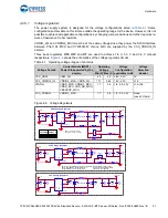
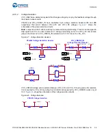
Page 39: ...ing set J14 to VCC_3V3 and remove jumper shunt from J26 VCC_VDDIO2_IN will also be 2 5 V if J16 is set to VCC_3V3 Figure 4 7 Voltage Selection Headers VCC_VDDIO0 voltage can be selected between VCC_3V3 and VCC_1V8 using zero ohm resistors It is connected to VCC_3V3 by default as microSD card powered by VCC_VDDIO0 works only at 3 3V Figure 4 8 shows the schematics of the voltage selection circuits ...

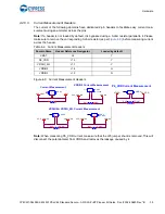
Page 40: ...8 Y P6_VDD J15 Y VDDIO_WL J17 Y VDDIO2 J18 N VDDIO0 J19 N Figure 4 9 Current Measurement Headers Note When measuring P6_VDD current make sure that the J25 jumper shunt is removed This will disconnect the potentiometer from VDDA and removes the leakage caused by it Table 4 2 Current Measurement Headers Domain Name Header Reference Designator Loaded by default R95 0 OHM No Load VBAT VCC_VBAT J8 HDR2...

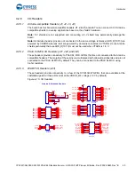
Page 41: ...They can be connected to the PSoC 64 MCU using 0 ohm resistors 4 2 6 3 WL BT I O Headers J23 These headers provide connectivity to a few of the CYW4343W GPIOs that are available at the castellated pads All these I Os work at the VDDIO_WL voltage 1 8 V by default Figure 4 10 I O Headers ARD_D0 ARD_D4 ARD_D3 ARD_D2 ARD_D1 ARD_D8 ARD_D7 ARD_D6 ARD_D5 ARD_D12 ARD_D11 ARD_D10 ARD_D9 ARD_D13 ARD_A1 ARD_...

Page 42: ... be reused as CSH For details on using CapSense including design guidelines see the Getting Started with CapSense Design Guide Figure 4 11 Schematics of CapSense Circuit Simultaneous GPIO switching with unrestricted drive strengths and frequency can affect CapSense and ADC performance For more details see the Errata section of the corresponding device datasheet CSB1 Tx 1 Rx 2 BTN_RX_SLD_TX CSB2 Tx...

Page 43: ... 64 MCU pins for user applications RGB R P1 1 RGB G P0 5 RGB B P7 3 LED O P1 5 LED R P11 1 Figure 4 12 LEDs Table 4 3 PSoC 64 pins for the LEDs User LED PSoC 64 MCU Pin O_LED_L R23 100 OHM R_LED_L R16 270 OHM P6_VDD R100 330 OHM User LEDs RGB_G_LED_L RGB_R_LED_L R G B LED5 RGB LED 1 2 3 4 RGB_B_LED_L R15 750 OHM R101 0 OHM VDDIO0 R22 1K LED9 RED LED8 ORANGE KitProg3 Status LED P5LP1_4 LED2 YELLOW ...

Page 44: ... a Cypress NOR flash memory S25FL512SAGMFI010 of 512Mb capacity The NOR flash is connected to the Quad SPI interface of the PSoC 64 MCU device The NOR flash device can be used for both data and code with execute in place XIP support and encryption Figure 4 14 Schematics of QSPI Flash SW4 EVQ PNF04M SW2 EVQ PNF04M USER_BTN_1 R20 10K User Button Hibernate Wakeup VBACKUP USER_BTN_2 VDDD R110 10K SW1 ...

Page 45: ... an SDHC interface but optionally can be connected using SPI by re working a few zero ohm resistors Figure 4 16 Schematics of microSD Card Section U4 CY15B104QSN CS 1 SO IO1 2 WP IO2 3 VSS 4 SI IO0 5 SCK 6 RESET IO3 7 VDD 8 Quad SPI F RAM FRAM_VDD FRAM_VDD FRAM_SS_L VCC_VDDIO0 FRAM_VDD C69 0 1uF 16V QSPI_SCK QSPI_IO0 QSPI_IO1 QSPI_IO2 QSPI_IO3 R113 10K R109 0 OHM TP10 R34 49 9K J20 MICROSD CARD SO...

Page 46: ...e P6_VDD power supply Remove jumper J25 to disconnect power from the potentiometer when measuring P6_VDD current Figure 4 18 Schematics of Potentiometer C60 22uF 25V P6_VBUS R103 100K USB Host VBUS Enable U18 AP2151WG 7 OUT 1 GND 2 FLG 3 EN 4 IN 5 P6_VDD VBUS_HOST VBUS_HOST Note P6_VBUS will be powered using KP_VBUS and hence will be limited in current based on other loads on the kit Please remove...

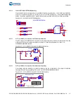
Page 47: ...connect the PSoC 64 MCU to trace header populate the resistors R126 R129 and remove resistors R117 R123 R125 Figure 4 20 ETM Trace Header 4 3 3 microSD Card Detect Multiplexing On the PSoC 64 MCU the default card detect pin for the SHDC block is P12 1 However on this kit P13 7 is connected to the card detect pin on the microSD card slot Therefore the firmware must be modified to use P13 7 as the c...

Page 48: ...4 24 U FL UMCC Connector for Antenna Diversity R34 49 9K J20 MICROSD CARD SOCKET DAT2 1 DAT3 2 CMD 3 VDD 4 CLK 5 VSS 6 DAT0 7 DAT1 8 CD1 9A CD_COM1 10A CD_COM2 10B CD2 9B R46 4 7K SD_CD_L VCC_VDDIO0 J_SD_DAT2 J_SD_DAT3 J_SD_CLK J_SD_DAT0 J_SD_DAT1 J_SD_CMD R169 0 OHM No Load R168 0 OHM R167 0 OHM No Load R166 0 OHM R164 0 OHM R165 0 OHM No Load J_SD_CMD J_SD_CLK J_SD_DAT0 R163 0 OHM R162 0 OHM SD_...

Page 49: ... 18 V The Kit can t be powered through the programming header J11 and has reverse voltage protection on this header 3 Why is the voltage of the kit restricted to 3 3 V Can t it drive external 5 V interfaces PSoC 64 MCU is not meant to be operated at voltages greater than 3 6 V Powering PSoC 64 MCU to more than 4 V will damage the chip It is recommended to power PSoC 64 MCU at 3 3 V 4 I am unable t...

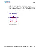
Page 50: ...1 and J12 However this can be by passed by loading R130 Note This modification is not recommended as the target MCU will have no protection and will be permanently damaged if 5V is supplied Figure 4 25 VTARG Reverse Voltage Protection R86 10K Q1 DMP2104LP 7 VTARG_REF VTARG R87 10K VTARG Reverse Voltage Protection R47 137K 1 Note VTARG_REF is only output voltage sense line for external debuggers PS...

Page 51: ...chapter on page 5 Removed description Added Regulatory Compliance Information on page 5 Updated Introduction chapter on page 7 Updated description Updated Getting Started on page 9 Updated description Updated Board Details on page 9 Updated description Updated Kit Operation chapter on page 18 Updated Theory of Operation on page 18 Updated description Updated Figure 2 1 Updated Figure 2 3 Updated F...

Page 52: ...tage Selection on page 38 Updated description Updated LEDs on page 42 Updated Table 4 3 Updated Cypress Quad SPI F RAM on page 44 Updated description Updated PSoC 64 Standard Secure AWS Wi Fi BT Pioneer Kit Rework on page 46 Updated U FL UMCC Connector for External Antenna on page 47 Updated description Updated Bill of Materials on page 48 Updated hyperlinks Updated Frequently Asked Questions on p...

Reviews: