


QUICK START GUIDE
EPC90132
EPC – POWER CONVERSION TECHNOLOGY LEADER |
| ©2021 |
| 3
Figure 3: Definition of dead-time between the upper-FET gate signal (DTQup)
and the lower-FET gate signal (DTQlow)
Figure 4: The required resistance values for R620 or R625 as a
function of desired dead-time
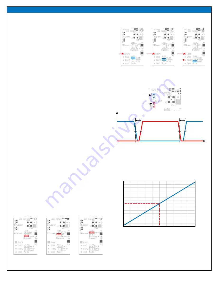
Figure 2: Input mode selection on J630
(a)
(c)
(b)
QUICK START PROCEDURE
The EPC90132 development board is easy to set up as a buck or boost
converter to evaluate the performance of two EPC2055 eGaN FETs.
This board includes a logic PWM input signal polarity changer used to ensure
positive PWM polarity for the switching device when configured in either
the buck or boost modes, and can accommodate both single and dual PWM
inputs. Furthermore, the board includes a dead-time generating circuit that
adds a delay from when the gate signal of one FET is commanded to turn
off, to when the gate signal of the other FET is commanded to turn on. In the
default configuration, this dead time circuit ensures that both the high and
low side FETs will not be turned on at the same time thus preventing a shoot-
through condition. The dead-time and/or polarity changing circuits can be
utilized or bypassed for added versatility.
Single/dual PWM signal input settings
There are two PWM signal input ports on the board, PWM1 and PWM2. Both
input ports are used as inputs in dual-input mode where PWM1 connects to
the upper FET and PWM2 connects to the lower FET. The PWM1 input port
is used as the input in single-input mode where the circuit will generate
the required complementary PWM for the FETs. The input mode is set by
choosing the appropriate jumper positions for J630 (mode selection) as
shown in figure 2(a) for a single-input buck converter (
blue
jumper across
pins 1 & 2 of J630), (b) for a single-input boost converter (
blue
jumpers
across pins 3 & 4 of J630), and (c) for a dual-input operation (
blue
jumpers
across pins 5 & 6 of J630).
Note
: In dual mode there is no shoot-through protection as both gate
signals can be set high at the same time.
Dead-time settings
Dead-time
is defined as the time between when one FET turns off and the
other FET turns on, and for this board is referenced to the input of the gate
driver. The dead-time can be set to a specific value where resistor R620
delays the turn on of the upper FET and resistor R625 delays the turn on of
the lower FET as illustrated in figure 3.
The required resistance for the desired dead-time setting can be read off
the graph in figure 4. An example for 10 ns dead-time setting shows that
a 120 Ω resistor is needed.
Note
: This is the default deadtime and resistor value installed. A minimum
dead-time of is 5 ns and maximum of 15 ns is recommended.
Bypass settings
Both the polarity changer and the deadtime circuits can be bypassed using
the jumper settings on J640 (Bypass), for direct access to the gate driver
input. There are three bypass options: 1) No bypass, 2) Dead-time bypass,
3) Full bypass. The jumper positions for J640 for all three bypass options are
shown in figure 5.
PWM1
Single input
Buck
Single input
Boost
Dual input
PWM2
R(Ω) = 13.5 ∙ DT(ns) − 14
Resistanc
e (Ω)
Dead-time (ns)
190
180
170
160
150
140
130
120
110
100
90
80
70
60
50
5
6
7
8
9
10
11
12
13
14
15
Figure 5: Bypass mode Jumper settings for J640
(a)
(c)
(b)
Deadtime
v
t
0
50%
50%
50%
50%
DTQup
DTQlow
Deadtime
Lower FET
turn on delay
Lower FET turn on delay
Upper FET
turn on delay
Upper FET turn on delay
No bypass
Bypass deadtime
Full Bypass


