background image


WAFER-AL SBC 


Page 2 

1.1 Introduction 


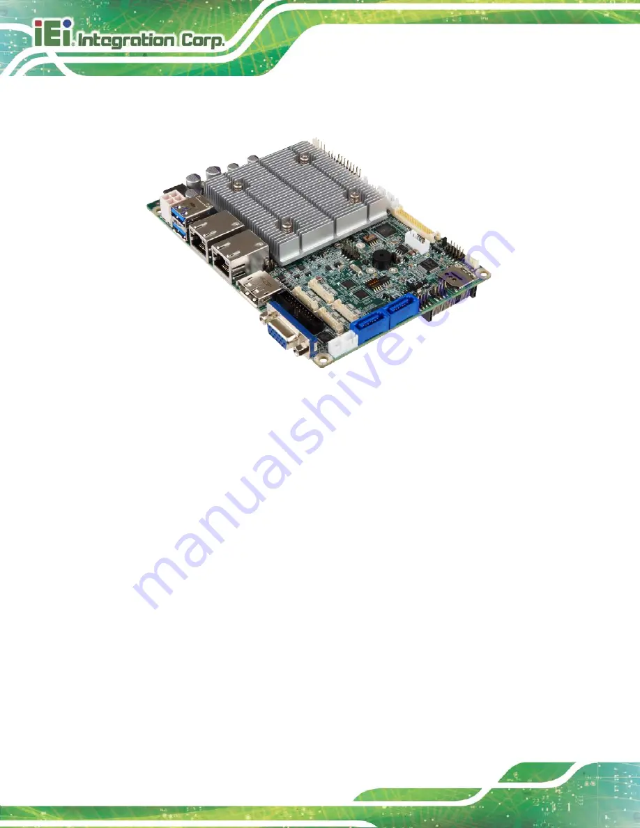
Figure 1-1: WAFER-AL 

The  WAFER-AL  series  is a  3.5”  single bard computer. It has an on-board 14nm  Intel

®


Pentium

®

  or  Celeron

®

  processor,  and supports one  204-pin  1867/1600 MHz 

single-channel DDR3 Low Voltage (DDR3L) SDRAM SO-DIMM slot with up to 8.0 GB of 

memory.   

The  WAFER-AL  series  includes  one DP++  connector, one VGA connector  and  one 

18-/24-bit  LVDS connector  for triple independent display.  Two  RJ-45  GbE  connectors 

provide the system with smooth connections to an external LAN. 

Expansion and I/O include one PCIe Mini slot supporting mSATA modules, one PCIe Mini 

slot  with SIM card holder,  two  USB  3.0  connectors  on the rear panel,  four  USB  2.0 

connectors by pin header and two SATA 6Gb/s connectors. Serial device connectivity is 

provided by two internal RS-232 connectors and two internal RS-232/422/485 connectors.   


Summary of Contents for WAFER-AL

Page 1: ...User Manual WAFER AL MODEL 3 5 SBC with 14nm Intel Pentium Celeron On board SoC DP VGA LVDS Dual PCIe GbE USB 3 0 PCIe Mini mSATA SATA 6Gb s RS 232 422 485 HD Audio SIM Slot and RoHS Rev 1 01 May 3 20...

Page 2: ...WAFER AL SBC Page II Revision Date Version Changes May 3 2018 1 01 Deleted E series SKUs Updated Chapter 6 Software Drivers November 30 2017 1 00 Initial release...

Page 3: ...sing out of the use or inability to use the product or documentation even if advised of the possibility of such damages This document contains proprietary information protected by copyright All rights...

Page 4: ...utionary messages should be heeded to help reduce the chance of losing data or damaging the product NOTE These messages inform the reader of essential but non critical information These messages shoul...

Page 5: ...13 3 CONNECTORS 14 3 1 PERIPHERAL INTERFACE CONNECTORS 15 3 1 1 WAFER AL Layout 15 3 1 2 Peripheral Interface Connectors 16 3 1 3 External Interface Panel Connectors 17 3 2 INTERNAL PERIPHERAL CONNECT...

Page 6: ...E CONNECTOR PANEL 42 3 3 1 DisplayPort Connector 42 3 3 2 LAN Connectors 44 3 3 3 USB Connectors 44 3 3 4 VGA Connector 45 4 INSTALLATION 47 4 1 ANTI STATIC PRECAUTIONS 48 4 2 INSTALLATION CONSIDERATI...

Page 7: ...71 5 3 ADVANCED 72 5 3 1 Trusted Computing 73 5 3 2 ACPI Settings 74 5 3 3 F81866 Super IO Configuration 75 5 3 3 1 Serial Port n Configuration 75 5 3 3 1 1 Serial Port 1 Configuration 76 5 3 3 1 2 S...

Page 8: ...ss Configuration 97 5 4 2 2 1 Onboard LAN 98 5 4 2 2 2 MINI PCIE 99 5 4 2 3 SATA Configuration 100 5 5 SECURITY 101 5 6 BOOT 102 5 7 SAVE EXIT 104 6 SOFTWARE DRIVERS 106 6 1 AVAILABLE DRIVERS 107 6 2...

Page 9: ...Connector Location 24 Figure 3 10 LVDS Connector Location 25 Figure 3 11 LAN LED Connector Locations 26 Figure 3 12 mSATA Module Slot Location 28 Figure 3 13 PCIe Mini Card Slot Location 29 Figure 3...

Page 10: ...Angle 54 Figure 4 8 Securing the Half size mSATA Module 54 Figure 4 9 Unlock SIM Card Slot Cover 55 Figure 4 10 SIM Card Installation 56 Figure 4 11 Lock SIM Card Slot Cover 56 Figure 4 12 AT ATX Mod...

Page 11: ...nouts 27 Table 3 12 LAN2 LED Connector JLAN_LED2 Pinouts 27 Table 3 13 mSATA Module Slot Pinouts 29 Table 3 14 PCIe Mini Card Slot Pinouts 30 Table 3 15 Power and HDD LED Connector Pinouts 31 Table 3...

Page 12: ...ct Switch Settings 57 Table 4 2 LVDS Voltage Select Jumper Settings 59 Table 4 3 LVDS Backlight Mode Select Jumper Settings 60 Table 4 4 LVDS Panel Resolution Selection 61 Table 4 5 RS 232 422 485 Mod...

Page 13: ...11 RTC Wake Settings 86 BIOS Menu 12 Power Saving Configuration 87 BIOS Menu 13 Serial Port Console Redirection 88 BIOS Menu 14 Legacy Console Redirection Settings 89 BIOS Menu 15 IEI Feature 90 BIOS...

Page 14: ......

Page 15: ...WAFER AL SBC Page 1 Chapter 1 1 Introduction...

Page 16: ...ne DP connector one VGA connector and one 18 24 bit LVDS connector for triple independent display Two RJ 45 GbE connectors provide the system with smooth connections to an external LAN Expansion and I...

Page 17: ...GHz dual core TDP 6 W DP LVDS iDP By order production MOQ 100 Table 1 1 WAFER AL Model Variations 1 3 Features Some of the WAFER AL motherboard features are listed below 3 5 motherboard supports 14nm...

Page 18: ...WAFER AL SBC Page 4 1 4 Connectors The connectors on the WAFER AL are shown in the figure below Figure 1 2 Connectors Front Side...

Page 19: ...WAFER AL SBC Page 5 Figure 1 3 Connectors Solder Side...

Page 20: ...WAFER AL SBC Page 6 1 5 Dimensions The dimensions of the WAFER AL series are listed in Figure 1 4 Figure 1 4 Dimensions with Heatsink mm...

Page 21: ...WAFER AL SBC Page 7 1 6 Data Flow Figure 1 5 shows the data flow between the system chipset the CPU and other components installed on the motherboard Figure 1 5 Data Flow Diagram...

Page 22: ...ting 4K codec decode encode for HEVC 4 H 264 VP8 SVC and MVC Display Output Triple independent display 1 x DP up to 4096x2160 60 Hz 1 x VGA up to 1920x1200 60 Hz 1 x 18 24 bit dual channel LVDS up to...

Page 23: ...wer connectors TPM 1 x TPM connector by 20 pin 2x10 header Expansion Two Full size Half size PCIe Mini card slots One supports mSATA module colay SATA2 One support SIM card holder Environmental and Po...

Page 24: ...WAFER AL SBC Page 10 Chapter 2 2 Unpacking...

Page 25: ...charge Self grounding Touch a grounded conductor every few minutes to discharge any excess static buildup Use an anti static pad When configuring any circuit board place it on an anti static mat Only...

Page 26: ...e IEI reseller or vendor the WAFER AL was purchased from or contact an IEI sales representative directly by sending an email to sales ieiworld com The WAFER AL is shipped with the following components...

Page 27: ...ay be separately purchased Item and Part Number Image RS 232 422 485 cable 250 mm p 1 25 P N 32005 003500 200 RS Dual USB port cable 210mm p 2 0 mm P N 32001 008600 200 RS Audio cable 300mm p 2 0 mm P...

Page 28: ...WAFER AL SBC Page 14 Chapter 3 3 Connectors...

Page 29: ...Connectors This chapter details all the jumpers and connectors 3 1 1 WAFER AL Layout The figures below show all the connectors and jumpers Figure 3 1 Connector and Jumper Locations Front Side Figure 3...

Page 30: ...r connector 5 pin wafer INV1 LVDS LCD connector 40 pin crimp LVDS1 LAN LED connectors 2 pin header JLAN_LED1 JLAN_LED2 Memory slot 204 pin SO DIMM DIMM1 mSATA module slot PCIe Mini slot MINI PCIE1 PCI...

Page 31: ...ader USB1 USB2 EC firmware update connector for internal use only 2 pin header CN5 Table 3 1 Peripheral Interface Connectors 3 1 3 External Interface Panel Connectors The table below lists the connect...

Page 32: ...1 12V DC IN Power Connector CN Label PWR1 CN Type 4 pin Molex p 4 2 mm CN Location See Figure 3 3 CN Pinouts See Table 3 3 The connector supports the 12V power supply Figure 3 3 12V DC IN Power Conne...

Page 33: ...ctor is connected to external audio devices including speakers and microphones for the input and output of audio signals to and from the system Figure 3 4 Audio Connector Location PIN NO DESCRIPTION P...

Page 34: ...ructions and local regulations NOTE It is recommended to attach the RTC battery onto the system chassis in which the WAFER AL is installed CN Label BT1 CN Type 2 pin wafer p 1 25 mm CN Location See Fi...

Page 35: ...r p 2 00 mm CN Location See Figure 3 6 CN Pinouts See Table 3 6 The 8 bit digital I O connector provides programmable input and output for external devices Figure 3 6 Digital I O Connector Location PI...

Page 36: ...CN Type 4 pin wafer p 2 54 mm CN Location See Figure 3 7 CN Pinouts See Table 3 7 The fan connector attaches to a cooling fan Figure 3 7 Fan Connector Location Pin Description 1 GND 2 V12S 3 Rotation...

Page 37: ...or supports HDMI LVDS VGA DVI and DisplayPort devices with up to 2560x1600 resolution The iDP connector is only available in iDP SKUs Figure 3 8 iDP Connector Location Pin Description Pin Description...

Page 38: ...er p 2 00 mm CN Location See Figure 3 9 CN Pinouts See Table 3 9 The backlight inverter connector provides power to an LCD panel Figure 3 9 Backlight Inverter Connector Location Pin Description 1 LCD_...

Page 39: ...or connected to the LVDS connector is set to 3 3 V by default To change the setting refer to Section 4 7 3 Figure 3 10 LVDS Connector Location Pin Description Pin Description 1 GROUND 2 GROUND 3 LVDS_...

Page 40: ...S_B_TX3 P 31 GROUND 32 GROUND 33 GROUND 34 GROUND 35 LCD VCC 36 LCD VCC 37 LCD VCC 38 LCD VCC 39 LCD VCC 40 LCD VCC Table 3 10 LVDS Connector Pinouts 3 2 9 LAN LED Connectors CN Label JLAN_LED1 JLAN_L...

Page 41: ...3 2 10 mSATA Module Slot CAUTION If an mSATA module is installed in the mSATA slot MINI PCIE1 the SATA port 2 SATA2 will be disabled Choose either the SATA2 connector or the mSATA module for storage C...

Page 42: ...C 11 PCIE_CLK 12 N C 13 PCIE_CLK 14 N C 15 GND 16 N C 17 N C 18 GND 19 N C 20 N C 21 GND 22 PCIRST 23 PCIE_RXN SATA_RX 24 N C 25 PCIE_RXP SATA_RX 26 GND 27 GND 28 1 5V 29 GND 30 SMBCLK 31 PCIE_TXN SAT...

Page 43: ...Location See Figure 3 13 CN Pinouts See Table 3 14 The PCIe Mini card slot is for installing a PCIe Mini expansion card with USB interface such as 3G modules Figure 3 13 PCIe Mini Card Slot Location...

Page 44: ...E_RXN 24 N C 25 PCIE_RXP 26 GND 27 GND 28 1 5V 29 GND 30 SMBCLK 31 PCIE_TXN 32 SMBDATA 33 PCIE_TXP 34 GND 35 GND 36 USBD 37 GND 38 USBD 39 VCC3 40 GND 41 VCC3 42 N C 43 GND 44 N C 45 N C 46 N C 47 N C...

Page 45: ...CN Location See Figure 3 14 CN Pinouts See Table 3 15 The CN1 connector connects to power and HDD LED indicators Figure 3 14 Power and HDD LED Connector Location Pin Description 1 VCC 5V 2 GND 3 PWR_...

Page 46: ...BTN1 CN Type 2 pin wafer p 2 00 mm CN Location See Figure 3 15 CN Pinouts See Table 3 16 The power button connector connects to a power button Figure 3 15 Power Button Connector Location Pin Descripti...

Page 47: ...T_BTN1 CN Type 2 pin wafer p 2 00 mm CN Location See Figure 3 16 CN Pinouts See Table 3 17 The reset button connector connects to a reset button Figure 3 16 Reset Button Connector Location Pin Descrip...

Page 48: ...1 25 mm CN Location See Figure 3 17 CN Pinouts See Table 3 18 The serial connectors provide RS 232 connection Figure 3 17 RS 232 Serial Port Connector Locations PIN NO DESCRIPTION PIN NO DESCRIPTION 1...

Page 49: ...he default mode is set to RS 232 by the on board switch To configure the connectors as RS 422 or RS 485 please refer to Section 4 7 6 Figure 3 18 RS 232 422 485 Connector Locations Pin RS 232 RS 422 R...

Page 50: ...RTS 8 CTS 9 RI Table 3 20 RS 232 422 485 Cable Pinouts 3 2 17 SATA 6Gb s Connectors CN Label SATA1 SATA2 CN Type 7 pin SATA connector CN Location See Figure 3 19 The SATA 6Gb s connector is connected...

Page 51: ...or or the mSATA module for storage 3 2 18 SATA Power Connectors CN Label SATA_PWR1 SATA_PWR2 CN Type 2 pin wafer p 2 00 mm CN Location See Figure 3 20 CN Pinouts See Table 3 21 The SATA power connecto...

Page 52: ...ccepts a micro SIM card for network communication Figure 3 21 SIM Card Slot Location 3 2 20 SMBus I2 C Connector CN Label J_SMB1 CN Type 4 pin wafer p 1 25 mm CN Location See Figure 3 22 CN Pinouts Se...

Page 53: ...2 21 SPI Flash Connector CN Label J_SPI1 CN Type 6 pin wafer p 1 25 mm CN Location See Figure 3 23 CN Pinouts See Table 3 23 The 6 pin SPI Flash connector is used to flash the BIOS Figure 3 23 SPI Fla...

Page 54: ...able 3 24 The Trusted Platform Module TPM connector secures the system on bootup Figure 3 24 TPM Connector Location Pin Description Pin Description 1 LCLK 2 GND 3 LFRAME 4 KEY 5 LRERST 6 5V 7 LAD3 8 L...

Page 55: ...mm CN Location See Figure 3 25 CN Pinouts See Table 3 25 These USB connectors provide four USB 2 0 ports by dual port USB cable Figure 3 25 USB Connector Locations PIN NO DESCRIPTION PIN NO DESCRIPTIO...

Page 56: ...rt connector 2 x GbE LAN connector 2 x USB 3 0 connector 1 x VGA connector Figure 3 26 External Peripheral Interface Connector 3 3 1 DisplayPort Connector CN Label DP1 CN Type DisplayPort CN Location...

Page 57: ...D GND 6 TMDS DATA1 L1N 7 TMDS DATA0 L2P 8 GND GND 9 TMDS DATA0 L2N 10 TMDS CLK L3P 11 GND GND 12 TMDS CLK L3N 13 DP_HDMI_SEL DP_HDMI_SEL 14 NC NC 15 SCL AUXP 16 GND GND 17 SDA AUXN 18 HDMI HPD DP HPD...

Page 58: ...iption 1 LAN_MDI0 7 LAN_MDI2 2 LAN_MDI0 8 LAN_MDI2 3 LAN_MDI1 9 LAN_MDI3 4 LAN_MDI1 10 LAN_MDI3 Table 3 27 LAN Pinouts Figure 3 28 LAN Connector 3 3 3 USB Connectors CN Label USB1 CN Type USB 3 0 port...

Page 59: ...DP1 15 USB3P0_RXDP2 7 GND 16 GND 8 USB3P0_TXDN1 17 USB3P0_TXDN2 9 USB3P0_TXDP1 18 USB3P0_TXDP2 Table 3 28 USB 3 0 Port Pinouts Figure 3 29 USB 3 0 Port Pinout Locations 3 3 4 VGA Connector CN Label VG...

Page 60: ...C Page 46 Figure 3 30 VGA Connector Pin Description Pin Description 1 RED 2 GREEN 3 BLUE 4 NC 5 GND 6 GND 7 GND 8 GND 9 VCC NC 10 GND 11 NC 12 DDC DAT 13 HSYNC 14 VSYNC 15 DDCCLK Table 3 29 VGA Connec...

Page 61: ...WAFER AL SBC Page 47 Chapter 4 4 Installation...

Page 62: ...help to prevent ESD from damaging the board Self grounding Before handling the board touch any grounded conducting material During the time the board is handled frequently touch any conducting materi...

Page 63: ...D from the body and helps prevent ESD damage Place the WAFER AL on an antistatic pad o When installing or configuring the motherboard place it on an antistatic pad This helps to prevent potential ESD...

Page 64: ...socket Step 3 Insert the SO DIMM Push the memory in at a 20 angle See Figure 4 1 Step 4 Seat the SO DIMM Gently push downwards and the arms clip into place See Figure 4 1 4 4 mSATA Module Installation...

Page 65: ...Mini slot MINI PCIE1 See Chapter 3 Step 2 Remove the retention screw as shown in Figure 4 2 Figure 4 2 Removing the Retention Screw Step 3 Line up the notch on the mSATA module with the notch on the s...

Page 66: ...igure 4 4 Securing the mSATA Module 4 4 2 Half size mSATA Module Installation To install a half size mSATA module please follow the steps below Step 1 Locate the PCIe Mini card slot MINI PCIE1 See Cha...

Page 67: ...Step 3 Install the previously removed standoff to the screw hole for the half size mSATA module Figure 4 6 Figure 4 6 Installing the Standoff Step 4 Line up the notch on the card with the notch on the...

Page 68: ...igure 4 7 Inserting the Half size mSATA Module into the Slot at an Angle Step 5 Secure the half size mSATA module with the retention screw previously removed Figure 4 8 Step 0 Figure 4 8 Securing the...

Page 69: ...ll a full size PCIe Mini card please refer to the steps described in Section 4 4 above 4 6 SIM Card Installation To install a SIM card please follow the steps below Step 1 Locate the SIM card slot See...

Page 70: ...the slot The cut mark on the corner should be facing away from the slot as shown in Figure 4 10 Figure 4 10 SIM Card Installation Step 4 Close the slot cover and lock it by sliding it in the direction...

Page 71: ...N Type Switch CN Location See Figure 4 12 CN Settings See Table 4 1 The AT ATX mode select switch specifies the systems power mode as AT or ATX AT ATX mode select switch settings are shown in Table 4...

Page 72: ...L fails to boot due to improper BIOS settings use the button to clear the CMOS data and reset the system BIOS information To clear the CMOS disconnect the battery BT1 and press the clear CMOS button f...

Page 73: ...nitor to select the correct voltage Jumper Label JP2 Jumper Type 3 pin header p 2 00 mm Jumper Settings See Table 4 2 Jumper Location See Figure 4 14 The LVDS voltage selection jumper allows setting t...

Page 74: ...mper Settings See Table 4 3 Jumper Location See Figure 4 15 The LVDS backlight mode selection jumper allows setting the mode of the LVDS backlight Setting Description Short 1 2 PWM mode Default Short...

Page 75: ...ription 0000 800x600 18 bit S default 0001 1024x768 18 bit S 0010 1024x768 24 bit S 0011 1280x768 18 bit S 0100 1280x800 18 bit S 0101 1280x960 18 bit S 0110 1280x1024 24 bit D 0111 1366x768 18 bit S...

Page 76: ...igure 4 17 The SW2 selects RS 232 422 485 mode of the COM1 and COM2 serial ports SW2 1 SW2 2 Description ON ON COM1 RS 422 ON OFF COM1 RS 232 Default OFF ON COM1 RS 485 SW2 3 SW2 4 Description ON ON C...

Page 77: ...he WAFER AL motherboard into the chassis please refer to the reference material that came with the chassis 4 9 Internal Peripheral Device Connections This section outlines the installation of peripher...

Page 78: ...nnect speakers to the line out audio jack Connect the output of an audio device to the line in audio jack Connect a microphone to the mic in audio jack Step 0 4 9 2 AT Power Connection Follow the inst...

Page 79: ...nnector to the AT power connector on the motherboard See Figure 4 19 Figure 4 19 Power Cable to Motherboard Connection Step 3 Connect Power Cable to Power Supply Connect one of the 4 pin 1x4 Molex typ...

Page 80: ...TA connector and the SATA power connector The locations of the connectors are shown in Chapter 3 Step 2 Insert the cable connector Insert the cable connector into the on board SATA drive connector and...

Page 81: ...Connect the cable to the SATA disk Connect the connector on the other end of the cable to the connector at the back of the SATA drive See Figure 4 21 Step 4 To remove the SATA cable from the SATA conn...

Page 82: ...WAFER AL SBC Page 68 Chapter 5 5 BIOS...

Page 83: ...LETE or F2 key as soon as the system is turned on or 2 Press the DELETE or F2 key when the Press Del to enter SETUP message appears on the screen 0 If the message disappears before the DELETE or F2 ke...

Page 84: ...ing the appropriate keys to use and the possible selections for the highlighted item appears To exit the Help Window press ESC or the F1 key again 5 1 4 Unable to Reboot after Configuration Changes If...

Page 85: ...09AR09 BIN Build Date and Time 01 09 2017 15 49 35 Platform firmware Information BXT SOC B1 MRC Version 0 56 PUNIT FW 24 PMC FW 03 26 TXE FW 3 0 11 1131 ISH FW 4 1 0 3364 GOP 0 0 0036 CPU Flavor BXT N...

Page 86: ...ttings made are compatible with the hardware Aptio Setup Utility Copyright C 2017 American Megatrends Inc Main Advanced Chipset Security Boot Save Exit Trusted Computing ACPI Settings F81866 Super IO...

Page 87: ...es BIOS support for security device O S will not show Security Device TCG EFI protocol and INT1A interface will not be available Select Screen Select Item EnterSelect F1 General Help F2 Previous Value...

Page 88: ...Select Change Opt F1 General Help F2 Previous Values F3 Optimized Defaults F4 Save Exit ESC Exit Version 2 18 1263 Copyright C 2017 American Megatrends Inc BIOS Menu 4 ACPI Settings ACPI Sleep State S...

Page 89: ...lues F3 Optimized Defaults F4 Save ESC Exit Version 2 18 1263 Copyright C 2017 American Megatrends Inc BIOS Menu 5 F81866 Super IO Configuration 5 3 3 1 Serial Port n Configuration Use the Serial Port...

Page 90: ...rupt address is IRQ4 IO 3F8h IRQ 3 4 Serial Port I O port address is 3F8h and the interrupt address is IRQ3 4 IO 2F8h IRQ 3 4 Serial Port I O port address is 2F8h and the interrupt address is IRQ3 4 I...

Page 91: ...rupt address is IRQ3 IO 3F8h IRQ 3 4 Serial Port I O port address is 3F8h and the interrupt address is IRQ3 4 IO 2F8h IRQ 3 4 Serial Port I O port address is 2F8h and the interrupt address is IRQ3 4 I...

Page 92: ...e the Change Settings option to change the serial port IO port address and interrupt address IO 3E8h IRQ 10 DEFAULT Serial Port I O port address is 3E8h and the interrupt address is IRQ10 IO 2E8h IRQ...

Page 93: ...e the Change Settings option to change the serial port IO port address and interrupt address IO 3E8h IRQ 10 Serial Port I O port address is 3E8h and the interrupt address is IRQ10 IO 2E8h IRQ 10 DEFAU...

Page 94: ...A CPU_CORE 0 712 V 5V 5 087 V 12V 12 144 V 5VSB 5 064 V 3 3V 3 456 V 3 3VSB 3 424 V Smart Fan Mode Select Select Screen Select Item EnterSelect Change Opt F1 General Help F2 Previous Values F3 Optimi...

Page 95: ...ge Opt F1 General Help F2 Previous Values F3 Optimized Defaults F4 Save Exit ESC Exit Version 2 18 1263 Copyright C 2017 American Megatrends Inc BIOS Menu 8 Smart Fan Mode Configuration CPU_FAN1 Smart...

Page 96: ...e fan duty cycle is 50 Use the or key to change the value or enter a decimal number between 1 and 100 5 3 5 USB Configuration Use the USB Configuration menu BIOS Menu 9 to read USB configuration infor...

Page 97: ...not enabled any attached USB mouse or USB keyboard does not become available until a USB compatible operating system is fully booted with all USB drivers loaded When this option is enabled any attach...

Page 98: ...2 L2 Cache 1024 KB x 1 L3 Cache Not Present 64 bit Supported EIST Enabled C States Disabled Intel Virtualization Technology Disabled VT d Disabled Enable Disable Intel SpeedStep Select Screen Select I...

Page 99: ...tem When combined with third party software Intel Virtualization technology allows several OSs to run on the same system at the same time Disabled DEFAULT Disables Intel Virtualization Technology Enab...

Page 100: ...Values F3 Optimized Defaults F4 Save ESC Exit Version 2 18 1263 Copyright C 2017 American Megatrends Inc BIOS Menu 11 RTC Wake Settings Wake system with Fixed Time Disabled Use the Wake system with F...

Page 101: ...on Power Saving Function Disabled Enable or Disable to reduce power consumption in system off state Select Screen Select Item EnterSelect F1 General Help F2 Previous Values F3 Optimized Defaults F4 Sa...

Page 102: ...rection Settings COM3 Console Redirection Disabled Console Redirection Settings COM4 Console Redirection Disabled Console Redirection Settings Legacy Console Redirection Legacy Console Redirection Set...

Page 103: ...M port to display redirection of Legacy OS and Legacy OPROM Messages Select Screen Select Item EnterSelect F1 General Help F2 Previous Values F3 Optimized Defaults F4 Save ESC Exit Version 2 18 1263 C...

Page 104: ...crashes Please install Auto Recovery API service before enabling this function Select Screen Select Item EnterSelect F1 General Help F2 Previous Values F3 Optimized Defaults F4 Save ESC Exit Version...

Page 105: ...BIOS menu may cause the system to malfunction Aptio Setup Utility Copyright C 2017 American Megatrends Inc Main Advanced Chipset Security Boot Save Exit North Bridge South Bridge North Bridge Paramete...

Page 106: ...Configuration Select Screen Select Item EnterSelect Change Opt F1 General Help F2 Previous Values F3 Optimized Defaults F4 Save Exit ESC Exit Version 2 17 1249 Copyright C 2017 American Megatrends Inc...

Page 107: ...Configuration Primary Display IGD Use the Primary Display option to select the graphics controller used as the primary boot device Select either an integrated graphics controller IGD or a PCI express...

Page 108: ...ect DVMT5 0 total graphic memory size used by the internal graphic device The following options are available 128M 256M MAX DEFAULT Primary IGFX Boot Display Auto Use the Primary IGFX Boot Display opt...

Page 109: ...t F1 General Help F2 Previous Values F3 Optimized Defaults F4 Save Exit ESC Exit Version 2 18 1263 Copyright C 2017 American Megatrends Inc BIOS Menu 19 South Bridge Configuration Restore on AC Power...

Page 110: ...ct Screen Select Item EnterSelect F1 General Help F2 Previous Values F3 Optimized Defaults F4 Save ESC Exit Version 2 18 1263 Copyright C 2017 American Megatrends Inc BIOS Menu 20 HD Audio Configurati...

Page 111: ...s Inc Chipset PCI Express Configuration Onboard LAN1 Onboard LAN2 MINI PCIE1 MINI PCIE2 Control the PCI Express Root Port Enable Enable PCIe root port Disable Disable PCIe root port Select Screen Sele...

Page 112: ...Express Root Port Enable Enable PCIe root port Disable Disable PCIe root port Select Screen Select Item EnterSelect F1 General Help F2 Previous Values F3 Optimized Defaults F4 Save ESC Exit Version 2...

Page 113: ...1 General Help F2 Previous Values F3 Optimized Defaults F4 Save ESC Exit Version 2 18 1263 Copyright C 2017 American Megatrends Inc BIOS Menu 23 MINI PCIE MINI PCIE1 MINI PCIE2 Enable Use the MINI PCI...

Page 114: ...ug Disabled SATA Port 1 Empty Hot Plug Disabled Determines how SATA controller s operate Select Screen Select Item EnterSelect F1 General Help F2 Previous Values F3 Optimized Defaults F4 Save ESC Exit...

Page 115: ...up and is only asked for when entering Setup If ONLY the User s password is set then this is a power on password and must be entered to boot or enter Setup In Setup the User will have Administrator ri...

Page 116: ...on 2 18 1263 Copyright C 2017 American Megatrends Inc BIOS Menu 26 Boot Bootup NumLock State On Use the Bootup NumLock State BIOS option to specify if the number lock setting must be modified during b...

Page 117: ...E Option ROMs Option ROM Messages Force BIOS Use the Option ROM Messages option to set the Option ROM display mode Force BIOS DEFAULT Sets display mode to force BIOS Keep Current Sets display mode to...

Page 118: ...erSelect F1 General Help F2 Previous Values F3 Optimized Defaults F4 Save ESC Exit Version 2 18 1263 Copyright C 2017 American Megatrends Inc BIOS Menu 27 Save Exit Save Changes and Reset Use the Save...

Page 119: ...Save as User Defaults Use the Save as User Defaults option to save the changes done so far as user defaults Restore User Defaults Use the Restore User Defaults option to restore the user defaults to...

Page 120: ...WAFER AL SBC Page 106 Chapter 6 6 Software Drivers...

Page 121: ...ownload Center https download ieiworld com Type WAFER AL and press Enter to find all the relevant software utilities and documentation Figure 6 1 IEI Resource Download Center IEI provides the followin...

Page 122: ...ER AL and press Enter Step 2 All product related software utilities and documentation will be listed You can choose Driver to filter the result Step 3 Click the driver file name on the page and you wi...

Page 123: ...to mount the file NOTE The Intel TXE requires that Microsoft s Kernel Mode Driver Framework KMDF version 1 11 update for Windows 7 must be installed first on Windows 7 OS If the KMDF is not installed...

Page 124: ...WAFER AL SBC Page 110 Appendix A A Regulatory Compliance...

Page 125: ...nce that may cause undesired operation This equipment has been tested and found to comply with the limits for a Class A digital device pursuant to part 15 of the FCC Rules These limits are designed to...

Page 126: ...WAFER AL SBC Page 112 B Product Disposal Appendix B...

Page 127: ...ed as electronic device in terms of the European Directive 2012 19 EU WEEE and must not be disposed of as domestic garbage EU wide legislation as implemented in each Member State requires that waste e...

Page 128: ...WAFER AL SBC Page 114 Appendix C C BIOS Menu Options...

Page 129: ...ettings IO 2E8h IRQ 10 79 PC Health Status 80 CPU_FAN1 Smart Fan Control Auto Duty Cycle Mode 81 CPU Temperature 1 81 CPU Temperature 2 82 CPU Temperature 3 82 CPU Temperature 4 82 USB Devices 83 Lega...

Page 130: ...CIe Speed Auto 99 STAT Controller Enable 100 SATA Mode Selection AHCI 100 Hot Plug Disabled 101 Administrator Password 101 User Password 101 Bootup NumLock State On 102 Quiet Boot Enabled 103 Launch P...

Page 131: ...WAFER AL SBC Page 117 Appendix D D Digital I O Interface...

Page 132: ...n off circuit of external devices or TTL devices Data can be read or written to the selected address to enable the DIO functions NOTE For further information please refer to the datasheet for the Supe...

Page 133: ...AH 6FH Sub function AL 9 Set the digital port as OUTPUT BL Digital I O output value Assembly Language Sample 2 MOV AX 6F09H setting the digital port as output MOV BL 09H digital value is 09H INT 15H D...

Page 134: ...WAFER AL SBC Page 120 Appendix E E Watchdog Timer...

Page 135: ...6FH Sub function AL 2 Sets the Watchdog Timer s period BL Time out value Its unit second is dependent on the item Watchdog Timer unit select in CMOS setup Table E 1 AH 6FH Sub function Call sub funct...

Page 136: ...deactivated the system will automatically restart after the Timer has finished its countdown EXAMPLE PROGRAM INITIAL TIMER PERIOD COUNTER W_LOOP MOV AX 6F02H setting the time out value MOV BL 30 time...

Page 137: ...WAFER AL SBC Page 123 Appendix F F Hazardous Materials Disclosure...

Page 138: ...hese components will be separately marked Please refer to the following table Part Name Toxic or Hazardous Substances and Elements Lead Pb Mercury Hg Cadmium Cd Hexavalent Chromium CR VI Polybrominate...

Page 139: ...BC Page 125 RoHS RoHS Pb Hg Cd CR VI PBB PBDE O O O O O O O O O O O O O O O O O O O O O O O O O O O O O O O O O O O O O O O O O O O O O O O O O SJ T 11363 2006 GB T 26572 2011 X SJ T 11363 2006 GB T 2...

Reviews: