IEI Technology PCISA-PV-D4251 User Manual Download Page 34


PCISA-PV-D4251/N4551/D5251 CPU Card 

Page 21

16 N/C 

41 HDD_RESET 

17 N/C 

42 IORDY 

18 SA2 

43 SDREQ 

19 SA1 

44 SDACK# 

20 SA0 

45 HDD_ACTIVE# 

21 DATA 

0  46 66DET 

22 DATA 

1  47 DATA 

23 DATA 

2  48 DATA 

24 N/C 

49 DATA 

10 

25 VCC-IN 

CHECK2 

50 GROUND 

Table 3-7: CF Card Socket Pinouts 

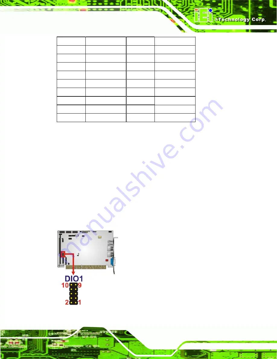
3.2.5 Digital Input/Output Connector 

CN Label: 

DIO1


CN Type: 

10-pin header (2x5) 

CN Location: 

See 

Figure 3-6


CN Pinouts: 

See 

Table 3-8


The DIO connector is managed through a Super I/O chip. The DIO connector pins are 

user programmable. The digital IO port of PCISA-PV-D4251/N4551/D5251 is 5V CMOS 

level.   


Figure 3-6: DIO Connector Location 


Summary of Contents for PCISA-PV-D4251

Page 1: ...D4251 N4551 D5251 CPU Card Page i IEI Technology Corp User Manual MODEL PCISA PV D4251 N4551 D5251 Half Size CPU Card for Intel Atom CPU DDR3 VGA LAN SATA 3Gb s USB HD Audio RoHS Compliant Rev 1 04 1...

Page 2: ...December 2012 1 03 Modified Table 3 18 Parallel Port Connector Pinouts Modified Section 2 4 Optional Items 25 July 2011 1 02 Modified Table 3 17 LVDS LCD Connector Pinouts 7 December 2010 1 01 Added m...

Page 3: ...damages arising out of the use or inability to use the product or documentation even if advised of the possibility of such damages This document contains proprietary information protected by copyright...

Page 4: ...ING LIST 12 2 4 OPTIONAL ITEMS 13 3 CONNECTORS 14 3 1 PERIPHERAL INTERFACE CONNECTORS 15 3 1 1 Layout 15 3 1 2 Peripheral Interface Connectors 15 3 1 3 External Interface Panel Connectors 17 3 2 INTER...

Page 5: ...R PANEL 36 3 3 1 CRT Connector 37 3 3 2 Ethernet Connectors 37 3 3 3 USB Connector 39 4 INSTALLATION 40 4 1 ANTI STATIC PRECAUTIONS 41 4 2 INSTALLATION CONSIDERATIONS 41 4 3 BASIC INSTALLATION 43 4 3...

Page 6: ...62 5 3 ADVANCED 63 5 3 1 Trusted Computing 63 5 3 2 CPU Configuration 64 5 3 3 SATA Configuration 66 5 3 4 USB Configuration 67 5 3 5 Super IO Configuration 68 5 3 5 1 Floppy Disk Controller Configura...

Page 7: ...efault Image 107 C 3 SETUP PROCEDURE FOR LINUX 112 C 4 RECOVERY TOOL FUNCTIONS 115 C 4 1 Factory Restore 117 C 4 2 Backup System 118 C 4 3 Restore Your Last Backup 119 C 4 4 Manual 120 C 5 OTHER INFOR...

Page 8: ...ion 23 Figure 3 9 Flash SPI ROM Connector Locations 24 Figure 3 10 Front Panel Connector Location 25 Figure 3 11 IDE Device Connector Location 26 Figure 3 12 Infrared Connector Pinout Locations 28 Fig...

Page 9: ...the Recovery Tool 101 Figure C 3 Recovery Tool Setup Menu 102 Figure C 4 Command Mode 102 Figure C 5 Partition Creation Commands 103 Figure C 6 Launching the Recovery Tool 105 Figure C 7 System Confi...

Page 10: ...C 25 Recovery Tool Menu 115 Figure C 26 Recovery Tool Main Menu 116 Figure C 27 Restore Factory Default 117 Figure C 28 Recovery Complete Window 117 Figure C 29 Backup System 118 Figure C 30 System Ba...

Page 11: ...9 Fan Connector Pinouts 23 Table 3 10 34 pin FDD Connector Pinouts 24 Table 3 11 Flash SPI ROM Connector Pinouts 25 Table 3 12 Front Panel Connector Pinouts 26 Table 3 13 IDE Connector Pinouts 27 Tabl...

Page 12: ...able 4 2 CF Card Setup Jumper Settings 46 Table 4 3 Clear CMOS Jumper Settings 47 Table 4 4 COM 2 Function Select Jumper Settings 48 Table 4 5 LVDS Voltage Selection Jumper Settings 50 Table 4 6 LVDS...

Page 13: ...enu 69 BIOS Menu 9 Serial Port n Configuration Menu 70 BIOS Menu 10 IrDA Configuration Menu 73 BIOS Menu 11 Parallel Port Configuration Menu 74 BIOS Menu 12 Hardware Health Configuration 76 BIOS Menu...

Page 14: ...PCISA PV D4251 N4551 D5251 CPU Card Page 1 Chapter 1 1 Introduction...

Page 15: ...d generation serial ATA SATA hard disk drives HDD with maximum transfer rates of 3Gb s and up to six USB 2 0 devices The PCISA PV D4251 N4551 D5251 also has a CompactFlash card socket for additional s...

Page 16: ...s include Powerful graphics Staying connected with both wired LAN connections Speedy running of multiple programs and applications 1 4 Features Some of the PCISA PV D4251 N4551 D5251 motherboard featu...

Page 17: ...PCISA PV D4251 N4551 D5251 CPU Card Page 4 1 5 Connectors The connectors on the PCISA PV D4251 N4551 D5251 are shown in the figure below Figure 1 2 Connectors Front Side...

Page 18: ...PCISA PV D4251 N4551 D5251 CPU Card Page 5 Figure 1 3 Connectors Solder Side...

Page 19: ...PCISA PV D4251 N4551 D5251 CPU Card Page 6 1 6 Dimensions The main dimensions of the PCISA PV D4251 N4551 D5251 are shown in the diagram below Figure 1 4 Dimensions mm...

Page 20: ...CISA PV D4251 N4551 D5251 CPU Card Page 7 1 7 Data Flow 5Figure 1 5 shows the data flow between the system chipset the CPU and other components installed on the motherboard Figure 1 5 Data Flow Diagra...

Page 21: ...400 MHz N455 Gen 3 5 DX9 200 MHz Integrated Graphics Analog CRT CRT hot plug supported D525 D425 up to 2048 x 1536 N455 up to 1400 x 1050 18 bit single channel LVDS supports up to WXGA 1366x768 or XG...

Page 22: ...DE One IDE connector via 44 pin box header Environmental and Power Specifications Power Supply AT ATX supported 5 V or 12 V by PCISA bus Power Consumption 12 V 0 57 A 5 V 3 36 A 1 8 GHz Intel Atom D52...

Page 23: ...PCISA PV D4251 N4551 D5251 CPU Card Page 10 Chapter 2 2 Packing List...

Page 24: ...discharge Self grounding Touch a grounded conductor every few minutes to discharge any excess static buildup Use an anti static pad When configuring any circuit board place it on an anti static mat On...

Page 25: ...rchased from or contact an IEI sales representative directly by sending an email to 32sales iei com tw The PCISA PV D4251 N4551 D5251 is shipped with the following components Quantity Item and Part Nu...

Page 26: ...on Guide Table 2 1 Packing List 2 4 Optional Items The following are optional components which may be separately purchased Item and Part Number Image CPU fan P N 19FTS00032100 000001 RS FDD cable P N...

Page 27: ...PCISA PV D4251 N4551 D5251 CPU Card Page 14 Chapter 3 3 Connectors...

Page 28: ...rs 3 1 1 Layout The figure below shows all the connectors and jumpers Figure 3 1 Connectors and Jumpers 3 1 2 Peripheral Interface Connectors The table below lists all the connectors on the board Conn...

Page 29: ...Mouse connector 6 pin wafer KB MS1 LCD backlight connector 5 pin wafer connector INV1 LVDS LCD connector 20 pin crimp connector LVDS1 Parallel port connector 26 pin header LPT1 RS 232 serial port con...

Page 30: ...rt connector USB_C1 USB 2 0 port 2 USB port connector USB_C2 Table 3 2 External Peripheral Connectors 3 2 Internal Peripheral Connectors The section describes all of the connectors on the PCISA PV D42...

Page 31: ...power mode settings are listed below PIN NO DESCRIPTION AT Mode Short 2 3 ATX Mode Use PS_ON and 5VSB cable Table 3 4 AT ATX Power Mode Setting 3 2 2 Audio Connector CN Label AUDIO1 CN Type 10 pin hea...

Page 32: ...Connector Pinouts 3 2 3 Battery Connector CN Label BAT1 CN Type 2 pin wafer 1x2 CN Location See Figure 3 4 CN Pinouts See Table 3 6 This is connected to the system battery The battery provides power t...

Page 33: ...to the CF socket on the solder side of the PCISA PV D4251 N4551 D5251 Figure 3 5 CF Card Socket Location PIN NO DESCRIPTION PIN NO DESCRIPTION 1 GROUND 26 VCC IN CHECK1 2 DATA 3 27 DATA 11 3 DATA 4 2...

Page 34: ...49 DATA 10 25 VCC IN CHECK2 50 GROUND Table 3 7 CF Card Socket Pinouts 3 2 5 Digital Input Output Connector CN Label DIO1 CN Type 10 pin header 2x5 CN Location See Figure 3 6 CN Pinouts See Table 3 8...

Page 35: ...ector CN Label CPU_FAN1 CN Type 4 pin wafer connector 1x4 CN Location See Figure 3 7 CN Pinouts See Table 3 9 The cooling fan connector provides a 12V 500mA current to a CPU cooling fan The connector...

Page 36: ...abel FDD1 CN Type 34 pin header 2x17 CN Location See Figure 3 8 CN Pinouts See Table 3 10 The floppy disk connector is connected to a floppy disk drive Figure 3 8 34 pin FDD Connector Location PIN NO...

Page 37: ...TRACK 0 27 GND 28 WRITE PROTECT 29 GND 30 READ DATA 31 GND 32 SIDE 1 SELECT 33 GND 34 DISK CHANGE Table 3 10 34 pin FDD Connector Pinouts 3 2 8 Flash SPI ROM Connector CN Label SPI1 CN Type 8 pin hea...

Page 38: ...Pinouts 3 2 9 Front Panel Connector CN Label F_PANEL1 CN Type 8 pin header 2x4 CN Location See Figure 3 10 CN Pinouts See Table 3 12 The front panel connector connects to several external switches an...

Page 39: ...nnector CN Label IDE1 CN Type 44 pin box header 2x22 CN Location See Figure 3 11 CN Pinouts See Table 3 13 One primary 44 pin IDE device connector on the PCISA PV D4251 N4551 D5251 supports connectivi...

Page 40: ...29 IDE DACK 30 GND 31 INT_IRQ14 32 N C 33 SDA1 34 IDE_PATADET 35 SDA0 36 SDA2 37 IDE CS1 38 IDE CS3 39 HDD ACTIVE 40 GND 41 VCC 42 VCC 43 GND 44 NC Table 3 13 IDE Connector Pinouts 3 2 11 Infrared Int...

Page 41: ...le 3 14 Infrared Connector Pinouts 3 2 12 Keyboard Mouse Connector CN Label KB MS1 CN Type 6 pin wafer 1x6 CN Location See Figure 3 13 CN Pinouts See Table 3 15 The keyboard mouse connector can be con...

Page 42: ...3 15 Keyboard Mouse Connector Pinouts 3 2 13 LCD Backlight Connector CN Label INV1 CN Type 5 pin wafer 1x5 CN Location See Figure 3 14 CN Pinouts See Table 3 16 The LCD backlight connector is for the...

Page 43: ...inouts See Table 3 17 The connector supports one or one channel 18 bit LVDS panel Figure 3 15 LVDS LCD Connector Location PIN NO DESCRIPTION PIN NO DESCRIPTION 1 GND 2 GND 3 LVDSA_DATA0 4 LVDSA_DATA 0...

Page 44: ...nnects to a parallel port connector interface or some other parallel port device such as a printer Figure 3 16 Parallel Port Connector Location PIN NO DESCRIPTION PIN NO DESCRIPTION 1 STB 2 AFD 3 PTD0...

Page 45: ...32 serial communications channel The COM1 COM3 and COM4 serial port connectors can be connected to external RS 232 serial port devices Figure 3 17 RS 232 Connector Pinout Locations PIN NO DESCRIPTION...

Page 46: ...e serial ports connectors connect to RS 232 422 485 serial port device Figure 3 18 COM2 Location PIN NO DESCRIPTION PIN NO DESCRIPTION 1 NDCDB 2 NDSRB 3 NSINB 4 NRTSB 5 NSOUTB 6 NCTSB 7 NDTRB 8 XRI2 9...

Page 47: ...ansfer data at speeds as high as 3Gb s Figure 3 19 SATA Drive Connector Locations PIN NO DESCRIPTION 1 GND 2 TXP 3 TXN 4 GND 5 RXN 6 RXP 7 GND Table 3 21 SATA Drive Connector Pinouts 3 2 19 SMBus Conn...

Page 48: ...SMBDATA 3 SMBCLK 4 5V Table 3 22 SMBus Connector Pinouts 3 2 20 USB Connectors Internal CN Label USB0_1 and USB0_2 CN Type 8 pin header 2x4 CN Location See Figure 3 21 CN Pinouts See Table 3 23 One 2...

Page 49: ...RIPTION 1 VCC 5V 2 GND 3 DATA 4 DATA 5 DATA 6 DATA 7 GND 8 VCC 5V Table 3 23 USB3 and USB4 Pinouts 3 3 External Peripheral Interface Connector Panel The figure below shows the external peripheral inte...

Page 50: ...A Connector PIN NO DESCRIPTION PIN NO DESCRIPTION 1 RED 2 GREEN 3 BLUE 4 N C 5 GND 6 GND 7 GND 8 GND 9 VCC 10 GND 11 N C 12 DDC DAT 13 HSYNC 14 VSYNC 15 DDC CLK Table 3 24 VGA Connector Pinouts 3 3 2...

Page 51: ...7 LAN _MDI2 16 GND 8 LAN _MDI2 17 NC 9 LAN _MDI3 18 NC Table 3 25 LAN1 and LAN2 Pinouts Figure 3 24 RJ 45 Ethernet Connector The RJ 45 Ethernet connector has two status LEDs one green and one yellow T...

Page 52: ...CN Label USB_C1 and USB_C2 CN Type USB port CN Location See Figure 3 22 CN Pinouts See Table 3 27 USB devices can be connected directly to the USB connectors on the rear panel PIN NO DESCRIPTION 1 VC...

Page 53: ...PCISA PV D4251 N4551 D5251 CPU Card Page 40 Chapter 4 4 Installation...

Page 54: ...ple anti static wristband can help to prevent ESD from damaging the board Self grounding Before handling the board touch any grounded conducting material During the time the board is handled frequentl...

Page 55: ...s prevent ESD damage Place the PCISA PV D4251 N4551 D5251 on an antistatic pad o When installing or configuring the motherboard place it on an antistatic pad This helps to prevent potential ESD damage...

Page 56: ...the socket Align the notch on the memory with the notch on the memory socket Step 3 Insert the SO DIMM Push the memory in at a 20 angle See Figure 4 1 Step 4 Seat the SO DIMM Gently push downwards and...

Page 57: ...allation To install the CPU card onto the backplane carefully align the CPU card edge connector with the CPU card socket on the backplane To do this please refer to the reference material that came wi...

Page 58: ...It consists of two or three metal pins and a small metal clip often protected by a plastic cover that slides over the pins to connect them To CLOSE SHORT a jumper means connecting the pins of the jump...

Page 59: ...p JP1 2 pin header Table 4 1 Jumpers 4 4 1 CF Card Setup Jumper Label JCF1 Jumper Type 2 pin header Jumper Settings See Table 4 2 Jumper Location See Figure 4 3 The CF Card Setup jumper sets the CF Ty...

Page 60: ...To do this use the jumper cap to close pins 2 and 3 for a few seconds then reinstall the jumper clip back to pins 1 and 2 If the CMOS Settings Wrong message is displayed during the boot up process th...

Page 61: ...4 4 Jumper Location See Figure 4 5 The COM 2 Function Select jumper sets the communication protocol used by the second serial communications port COM 2 as RS 232 RS 422 or RS 485 The COM 2 Function Se...

Page 62: ...ected with this jumper Please refer to the user guide that cam with the monitor to select the correct voltage Jumper Label J_VLVDS1 Jumper Type 6 pin header Jumper Settings See Table 4 5 Jumper Locati...

Page 63: ...per Label JP3 Jumper Type 6 pin header Jumper Settings See Table 4 6 Jumper Location See Figure 4 7 The LVDS Panel Resolution Selection jumper allows the LVDS screen resolution to be set The LVDS Pane...

Page 64: ...lection jumper location is shown in Figure 4 7 Figure 4 7 LVDS Resolution Selection Jumper Pinout Locations 4 4 6 PCIe Interface Setup Jumper Label JP1 Jumper Type 2 pin header Jumper Settings See Tab...

Page 65: ...nnection The PCISA PV D4251 N4551 D5251 is shipped with three SATA drive cables To connect the SATA drives to the connectors please follow the steps below Step 1 Locate the connectors The locations of...

Page 66: ...ction Step 3 Connect the cable to the SATA disk Connect the connector on the other end of the cable to the connector at the back of the SATA drive See Figure 4 10 Step 4 Connect the SATA power cable C...

Page 67: ...cable To connect the USB cable connector please follow the steps below Step 1 Locate the connectors The locations of the USB connectors are shown in Chapter 3 WARNING If the USB pins are not properly...

Page 68: ...ssis The USB 2 0 connectors are attached to a bracket To secure the bracket to the chassis please refer to the installation instructions that came with the chassis Step 0 4 6 External Peripheral Inter...

Page 69: ...n Step 3 Insert the LAN cable RJ 45 connector Once aligned gently insert the LAN cable RJ 45 connector into the on board RJ 45 connector Step 0 4 6 2 USB Device Connection There are two external USB 2...

Page 70: ...CRT or VGA monitor To connect a monitor to the PCISA PV D4251 N4551 D5251 please follow the instructions below Step 1 Locate the female DB 15 connector The location of the female DB 15 connector is s...

Page 71: ...or the PCISA PV D4251 N4551 D5251 are on the CD that came with the system To install the drivers please follow the steps below Step 1 Insert the CD into a CD drive connected to the system NOTE If the...

Page 72: ...PCISA PV D4251 N4551 D5251 CPU Card Page 59 Chapter 5 5 BIOS...

Page 73: ...to enter SETUP message appears on the screen 0 If the message disappears before the F2 key is pressed restart the computer and try again 5 1 2 Using Setup Use the arrow keys to highlight items press...

Page 74: ...1 4 Unable to Reboot After Configuration Changes If the computer cannot boot after changes to the system configuration is made CMOS defaults Use the jumper described in Chapter 4 5 1 5 BIOS Menu Bar...

Page 75: ...et the Time Use Tab to switch between Time elements Select Screen Select Item EnterSelect F1 General Help F2 Previous Values F3 Optimized Defaults F4 Save ESC Exit Version 2 01 1204 Copyright C 2010 A...

Page 76: ...hardware Aptio Setup Utility Copyright C 2010 American Megatrends Inc Main Advanced Chipset Boot Security Save Exit Trusted Computing CPU Configuration SATA Configuration USB Configuration Super IO Co...

Page 77: ...red Select Screen Select Item EnterSelect F1 General Help F2 Previous Values F3 Optimized Defaults F4 Save ESC Exit Version 2 01 1204 Copyright C 2010 American Megatrends Inc BIOS Menu 3 TPM Configura...

Page 78: ...ght C 2010 American Megatrends Inc BIOS Menu 4 CPU Configuration The CPU Configuration menu BIOS Menu 4 lists the following CPU details Processor Type Lists the brand name of the CPU being used EMT64...

Page 79: ...General Help F2 Previous Values F3 Optimized Defaults F4 Save ESC Exit Version 2 01 1204 Copyright C 2010 American Megatrends Inc BIOS Menu 5 IDE Configuration ATA IDE Configurations Enhanced Use the...

Page 80: ...Utility Copyright C 2010 American Megatrends Inc Advanced USB Configuration USB Devices 1 Keyboard 2 Hubs Legacy USB Support Enabled Enables Legacy USB support AUTO option disables legacy support if n...

Page 81: ...SB support disabled if no USB devices are connected 5 3 5 Super IO Configuration Use the Super IO Configuration menu BIOS Menu 7 to set or change the configurations for the FDD controllers parallel po...

Page 82: ...d Device Settings Reset Required Enable or Disable Floppy Disk Controller Select Screen Select Item EnterSelect F1 General Help F2 Previous Values F3 Optimized Defaults F4 Save ESC Exit Version 2 01 1...

Page 83: ...ues F3 Optimized Defaults F4 Save ESC Exit Version 2 01 1204 Copyright C 2010 American Megatrends Inc BIOS Menu 9 Serial Port n Configuration Menu 5 3 5 2 1 Serial Port 0 Configuration Serial Port Ena...

Page 84: ...Settings Auto Use the Change Settings option to change the serial port IO port address and interrupt address Auto DEFAULT The serial port IO port address and interrupt address are automatically detec...

Page 85: ...8h IRQ 10 11 Serial Port I O port address is 3E8h and the interrupt address is IRQ10 11 IO 2E8h IRQ 10 11 Serial Port I O port address is 2E8h and the interrupt address is IRQ10 11 5 3 5 2 4 Serial Po...

Page 86: ...menu BIOS Menu 9 to configure the serial port n Aptio Setup Utility Copyright C 2010 American Megatrends Inc Advanced IrDA Configuration IrDA Enabled Device Settings Reset Required Enable or Disable I...

Page 87: ...lts F4 Save ESC Exit Version 2 01 1204 Copyright C 2010 American Megatrends Inc BIOS Menu 11 Parallel Port Configuration Menu Parallel Port Enabled Use the Parallel Port option to enable or disable th...

Page 88: ...IO 3BCh Parallel Port I O port address is 3BCh Device Mode Printer Mode Use the Device Mode option to select the mode the parallel port operates in Configuration options are listed below Printer Mode...

Page 89: ...d1 60 Temperature Bound2 50 Temperature Bound3 40 Temperature Bound4 30 Select Screen Select Item EnterSelect F1 General Help F2 Previous Values F3 Optimized Defaults F4 Save ESC Exit Version 2 01 120...

Page 90: ...by re directing keyboard input and text output through the serial port Aptio Setup Utility Copyright C 2010 American Megatrends Inc Advanced COM0 Console Redirection Disabled Console Redirection Setti...

Page 91: ...wrong values for the Chipset BIOS selections in the Chipset BIOS menu may cause the system to malfunction Aptio Setup Utility Copyright C 2010 American Megatrends Inc Main Advanced Chipset Boot Secur...

Page 92: ...aphics controller to use as the primary boot device Select Screen Select Item EnterSelect F1 General Help F2 Previous Values F3 Optimized Defaults F4 Save ESC Exit Version 2 01 1204 Copyright C 2010 A...

Page 93: ...ptimized Defaults F4 Save ESC Exit Version 2 01 1204 Copyright C 2010 American Megatrends Inc BIOS Menu 16 OnChip VGA Configuration Share Memory Size 8 MB Use the Share Memory Size option to set the a...

Page 94: ...ion Disabled HD Audio Controller Select Screen Select Item EnterSelect F1 General Help F2 Previous Values F3 Optimized Defaults F4 Save ESC Exit Version 2 01 1204 Copyright C 2010 American Megatrends...

Page 95: ...spread spectrum mode is enabled 5 4 3 Intel IGD SWSCI OpRegion Use the Intel IGD SWSCI OpRegion menu to configure the video device connected to the system Aptio Setup Utility Copyright C 2010 American...

Page 96: ...IXED Memory option to specify the maximum amount of memory that can be allocated as graphics memory Configuration options are listed below 128 MB 256 MB Default Maximum IGD Boot Type VBIOS Default Use...

Page 97: ...ct the keyboard NumLock state Select Screen Select Item EnterSelect F1 General Help F2 Previous Values F3 Optimized Defaults F4 Save ESC Exit Version 2 01 1204 Copyright C 2010 American Megatrends Inc...

Page 98: ...play when the system boots Disabled Normal POST messages displayed Enabled DEFAULT OEM Logo displayed instead of POST messages Fast Boot Disabled Use the Fast Boot option to enable or disable boot wit...

Page 99: ...LY the User s password is set then this is a power on password and must be entered to boot or enter Setup In Setup the User will have Administrator rights Administrator Password User Password Set Setu...

Page 100: ...Item EnterSelect F1 General Help F2 Previous Values F3 Optimized Defaults F4 Save ESC Exit Version 2 01 1204 Copyright C 2010 American Megatrends Inc BIOS Menu 21 Exit Save Changes and Reset Use the...

Page 101: ...ard Page 88 Save as User Defaults Use the Save as User Defaults option to save the changes done so far as user defaults Restore User Defaults Use the Restore User Defaults option to restore the user d...

Page 102: ...PCISA PV D4251 N4551 D5251 CPU Card Page 89 Appendix A A BIOS Options...

Page 103: ...Port Enabled 71 Change Settings Auto 71 Serial Port Enabled 71 Change Settings Auto 72 Serial Port Enabled 72 Change Settings Auto 72 IrDA Enabled 73 Parallel Port Enabled 74 Change Settings Auto 74...

Page 104: ...Select by Panel ID 83 Bootup NumLock State On 84 Quiet Boot Enabled 85 Fast Boot Disabled 85 Launch PXE OpROM Disabled 85 Administrator Password 86 User Password 86 Save Changes and Reset 87 Discard C...

Page 105: ...PCISA PV D4251 N4551 D5251 CPU Card Page 92 Appendix B B Terminology...

Page 106: ...Input Output System BIOS is firmware that is first run when the computer is turned on and can be configured by the end user CODEC The Compressor Decompressor CODEC encodes and decodes digital audio d...

Page 107: ...fers data at 1 0 Gbps and complies with the IEEE 802 3 2005 standard GPIO General purpose input HDD Hard disk drive HDD is a type of magnetic non volatile computer storage device that stores digitally...

Page 108: ...sis and Reporting Technology S M A R T refers to automatic status checking technology implemented on hard disk drives UART Universal Asynchronous Receiver transmitter UART is responsible for asynchron...

Page 109: ...PCISA PV D4251 N4551 D5251 CPU Card Page 96 Appendix C C One Key Recovery...

Page 110: ...Recovery tool as shown in Figure C 1 to backup or restore Windows system five setup procedures are required 1 Hardware and BIOS setup see Section C 2 1 2 Create partitions see Section C 2 2 3 Install...

Page 111: ...e for the operating system while the second partition will be invisible to the operating system and contain the backup made by the one key recovery software The partition created for recovery images m...

Page 112: ...upported OS versions are listed below Microsoft Windows o Windows XP Service Pack 2 or 3 required o Windows Vista o Windows 7 o Windows CE 5 0 o Windows CE 6 0 o Windows XP Embedded Linux o Fedora Cor...

Page 113: ...ery partition see Section C 2 4 Step 5 Create factory default image see Section C 2 5 S t e p 0 The detailed descriptions are described in the following sections NOTE The setup procedures described be...

Page 114: ...t e p 0 C 2 2 Create Partitions To create the system backup the main storage device must be split into two partitions three partitions for Linux The first partition will be for the operating system w...

Page 115: ...ollowing commands marked in red to create two partitions One is for the OS installation the other is for saving recovery files and images which will be an invisible partition Press Enter after enterin...

Page 116: ...PCISA PV D4251 N4551 D5251 CPU Card Page 103 system32 format F fs ntfs q v Recovery y system32 exit Figure C 5 Partition Creation Commands...

Page 117: ...g system onto the unlabelled partition The partition labeled as Recovery is for use by the system recovery tool and should not be used for installing the operating system or any applications NOTE The...

Page 118: ...y key to boot from the recovery CD It will take a while to launch the recovery tool Please be patient Figure C 6 Launching the Recovery Tool Step 4 When the recovery tool setup menu appears press 2 th...

Page 119: ...hidden and the recovery tool is saved in this partition Figure C 8 Build up Recovery Partition Step 6 After completing the system configuration press any key in the following window to reboot the sys...

Page 120: ...follow the steps below Step 1 Turn on the system When the following screen displays Figure C 10 press the F3 key to access the recovery tool The message will display for 10 seconds please press F3 be...

Page 121: ...rd Page 108 Figure C 12 About Symantec Ghost Window Step 4 Use mouse to navigate to the option shown below Figure C 13 Figure C 13 Symantec Ghost Path Step 5 Select the local source drive Drive 1 as s...

Page 122: ...shown in Figure C 15 Then click OK Figure C 15 Select a Source Partition from Basic Drive Step 7 Select 1 2 Recovery NTFS drive and enter a file name called iei Figure C 16 Click Save The factory defa...

Page 123: ...V D4251 N4551 D5251 CPU Card Page 110 Figure C 16 File Name to Copy Image to Step 8 When the Compress Image screen in Figure C 17 prompts click High to make the image file smaller Figure C 17 Compress...

Page 124: ...re C 18 Image Creation Confirmation Step 10 The Symantec Ghost starts to create the factory default image Figure C 19 Figure C 19 Image Creation Complete Step 11 When the image creation completes a sc...

Page 125: ...indows Please follow the steps below to setup recovery tool for Linux OS Step 1 Hardware and BIOS setup Refer to Section C 2 1 Step 2 Install Linux operating system Make sure to install GRUB v0 97 or...

Page 126: ...art DISKPART list vol DISKPART sel disk 0 DISKPART create part pri size ___ DISKPART assign letter N DISKPART exit system32 format N fs ntfs q v Recovery y system32 exit Step 4 Build up recovery parti...

Page 127: ...recovery tool main menu by modifying the menu lst To first access the recovery tool main menu the menu lst must be modified In Linux system enter Administrator root When prompt appears type cd boot g...

Page 128: ...reate a factory default image Follow Step 2 Step 12 described in Section C 2 5 to create a factory default image C 4 Recovery Tool Functions After completing the initial setup procedures as described...

Page 129: ...be saved in the hidden partition 8 Restore your last backup Restore the last system backup image 9 Manual Enter the Symantec Ghost window to configure manually 10 Quit Exit the recovery tool and rest...

Page 130: ...Enter in the main menu Step 2 The Symantec Ghost window appears and starts to restore the factory default A factory default image called iei GHO is created in the hidden Recovery partition Figure C 2...

Page 131: ...n the main menu Step 2 The Symantec Ghost window appears and starts to backup the system A backup image called iei_user GHO is created in the hidden Recovery partition Figure C 29 Backup System Step 3...

Page 132: ...w Step 1 Type 3 and press Enter in the main menu Step 2 The Symantec Ghost window appears and starts to restore the last backup image iei_user GHO Figure C 31 Restore Backup Step 3 The screen is shown...

Page 133: ...follow the steps below Step 1 Type 4 and press Enter in the main menu Step 2 The Symantec Ghost window appears Use the Ghost program to backup or recover the system manually Figure C 33 Symantec Ghos...

Page 134: ...ing one key recovery Please follow the steps below to install the SATA RAID AHCI driver Step 1 Copy the SATA RAID AHCI driver to a floppy disk and insert the floppy disk into a USB floppy disk drive T...

Page 135: ...d Page 122 Step 5 When the following window appears press S to select Specify Additional Device Step 6 In the following window select a SATA controller mode used in the system Then press Enter The use...

Page 136: ...m Step 4 in Section C 2 2 Create Partitions to finish the whole setup process S t e p 0 C 5 2 System Memory Requirement To be able to access the recovery tool by pressing F3 while booting up the syste...

Page 137: ...PCISA PV D4251 N4551 D5251 CPU Card Page 124 Appendix D D Watchdog Timer...

Page 138: ...r INT 15H AH 6FH Sub function AL 2 Sets the Watchdog Timer s period BL Time out value Its unit second is dependent on the item Watchdog Timer unit select in CMOS setup Table D 1 AH 6FH Sub function Ca...

Page 139: ...imer is not deactivated the system will automatically restart after the Timer has finished its countdown EXAMPLE PROGRAM INITIAL TIMER PERIOD COUNTER W_LOOP MOV AX 6F02H setting the time out value MOV...

Page 140: ...PCISA PV D4251 N4551 D5251 CPU Card Page 127 Appendix E E Digital I O Interface...

Page 141: ...bit7 as Input value mov dx 0A21h GPIO output I O base address in al dx Get output status jmp 2 Wait jmp 2 Wait and al 0Fh mov bl al Move al to bl temporarily inc dx sets dx to 0A22h in al dx Get inpu...

Page 142: ...PCISA PV D4251 N4551 D5251 CPU Card Page 129 Appendix F F Hazardous Materials Disclosure...

Page 143: ...es the presences of small quantities of certain materials in the product and is applicable to China RoHS only A label will be placed on each product to indicate the estimated Environmentally Friendly...

Page 144: ...Circuit Board X O O O O X Metal Fasteners X O O O O O Cable Assembly X O O O O X Fan Assembly X O O O O X Power Supply Assemblies X O O O O X Battery O O O O O O O This toxic or hazardous substance i...

Page 145: ...A PV D4251 N4551 D5251 CPU Card Page 132 RoHS RoHS Pb Hg Cd CR VI PBB PBDE X O O O O X X O O O O X X O O O O X X O O O O O X O O O O X X O O O O X X O O O O X O O O O O O O SJ T11363 2006 X SJ T11363...

Reviews: