12. Register Descriptions
317
PowerSpan II User Manual
80A1010_MA001_09
Integrated Device Technology
www.idt.com
12.5.40
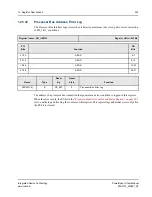
DMA x Attributes Register
This register contains additional parameters for DMA channel x. It is not part of a Linked-List
Command Packet.
Register Name: DMAx_ATTR
Register Offset: 0x324, 0x354, 0x384, 0x3B4
PCI
Bits
Function
PB
Bits
31-24
CP_PORT
0
GBL_
CI_
PowerSpan II Reserved
0-7
23-16
PowerSpan II Reserved
RTT
8-15
15-08
PowerSpan II Reserved
WTT
16-23
07-00
PowerSpan II Reserved
24-31
Name
Type
Reset
By
Reset
State
Function
CP_PORT
[1:0]
R/W
G_RST
0
Command Packet Port
00 = PCI-1
01 = PCI-2,
10 = PB
11 = reserved
Single PCI PowerSpan II:
00 = PCI-1
10 = PB
01, 11 = reserved
PB_GBL_
R/W
G_RST
0
Processor Bus Global
0 = Assert PB_GBL_
1 = Negate PB_GBL_
PB_CI_
R/W
G_RST
0
Processor Bus Cache Inhibit
0 = Assert PB_CI_
1 = Negate PB_CI_
RTT[4:0]
R/W
G_RST
01010
Processor Bus Read Transfer Type PB_TT[0:4]
Selects the Transfer Type on the Processor Bus. The register
bits RTT[4:0]/WTT[4:0] are mapped to pins PB_TT[0:4].
01010 = Read
WTT[4:0]
R/W
G_RST
00010
Processor Bus Write Transfer Type PB_TT[0:4]
Selects the Transfer Type on the Processor Bus. The register
bits RTT[4:0]/WTT[4:0] are mapped to pins PB_TT[0:4].
00010 = Write with flush


