P9038 LAYOUT GUIDE
12
08/23/15
AN-894
Noise-sensitive Circuits
The sensitive circuits refer to noise sensitive circuits that should be referenced to GND on the side of the P9038 that is furthest
from the PGND pins and input capacitors ("Quiet GND" side). They include the Input current sense filters (previously discussed),
the ISNS_AVG pin (pin 48 for the QFN) connection to capacitor (C47), the LDO pins and filter capacitors, VSNS_AVG (Pin24)
plus capacitor C51, REFGND (pin 17) and the DEMOD WPC communication filters. The most important guidance with respect
to layout for all of these sensitive circuits is to tie them to GND on the opposite side of the IC from the PGND pins.
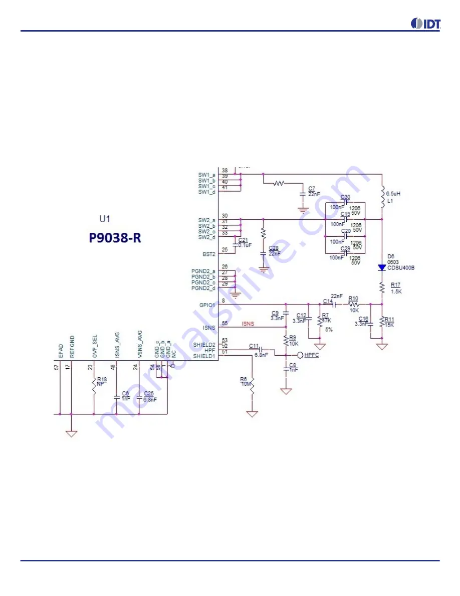
Figure 10. P9038 DEMOD Communication Filters and Accompanying Components
Note: not all pins are shown in the figure)
shows all of the components considered part of the DEMOD filters connected to the Tx coil, along with a few other
sensitive components and pins. The optimal layout will have the anode of diode D6 placed close to the LC resonance node, and
the remaining DEMOD filter components adjacent to the P9038 device in the 'Quiet' GND area. The connection from the cathode
of D6 to R17 is subject to periodic high voltage surges near 50V-peak and should be given at least 10 mils of clearance from any
other net or connection. Resistors R6 and the connections to SHEILD1 (pin 51) should be kept in close proximity and use the
same GND connection as the point where C8 is merged with the rest of the GND circuits (in the 'Quiet' GND area). The input
connection from C11 to the HPF (pin 52) is high impedance and is the most noise sensitive pin on the device. Extra care must
be taken to route connections from HPF to C11 & C8 / R9. ISNS to C9 trace lengths should be minimized and avoid routing near
PGND and VIN or SW1 and SW2 switching signals that exist on the PCB.


