background image

08/23/15

11

P9038 LAYOUT GUIDE

AN-894  

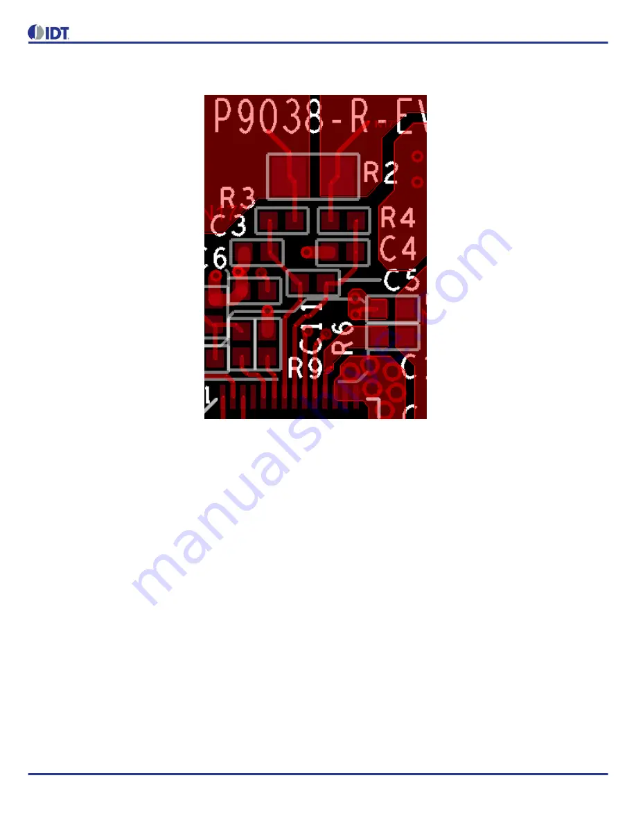
Figure 9. Kelvin Connections to Rsns (R40)

The Input power connections and traces should be routed with adequate width to conduct up to 2 A of DC current with minimal 
voltage losses. When using the USB and N-CH FET, a device with an acceptable and minimal RDSON specification should be 
selected. 

The High Current Power GND will carry the DC input current up to ~ 1.7 A, including the input ripple current at the power transfer 
frequency. As a result, it may be prone to varying voltage drops depending on the Rx load and is not recommended to be 
common to sensitive GND for DEMOD signals. The Noisy PGND area will have high current switching and rapid voltage changes 
induced from the full bridge inverter switching, this area is not suitable to be used for GND reference. The DEMOD circuits GND 
connections should be made away from the PGND pins and have a separate current return path to the EPAD from the input 
capacitors and the PGND pins. 

Next, the LDO input capacitors need to be placed in close proximity to the P9038 device. The P9038 has two Low Drop-Out 
(LDO) linear voltage regulators: LDO5V (Pin 19), LDO2P5V (Pin 20). The LDO5V output and LDO2P5V input may share a single 
1µF ceramic capacitor for cost reduction or compact designs. Both LDO input and output capacitors should be placed near each 
respective LDO pin with the GND plate of the capacitor connected to the EPAD GND area of the PCB. While the LDO's are 
technically power circuits, they are sensitive to noise and should not be placed far from the P9038 device to promote stable and 
reliable operation.

EPAD

The use of a grid of 25 thermal vias placed inside the E-PAD of the P9038 device is recommended. Using thermal vias and 
having one or more GND planes in direct contact is crucial for optimal thermal performance. Typical thermal via diameter is 
0.3mm and spacing should be 1mm pitch. The land pattern drawing can be found in the product datasheet.


Summary of Contents for P9038

Page 1: ... Reference Layout 2 Importing the Reference Layout 2 Connecting a Power Source 3 Connecting Inputs Outputs 3 Manufacturing Notes 3 Additional Resources 3 Custom Layout Guidelines 4 Layout Priority Checklist 4 Power Circuits 5 Input Capacitors 7 BST and ZVS Capacitors 9 EPAD 11 Noise sensitive Circuits 12 Non sensitive Circuits 13 PCB Footprint Design 13 Thermal Performance 14 ...

Page 2: ...e by following these instructions 1 Use or copy the P9038 R EVK schematic file dsn and export the netlist to a PCB file 2 Move the file P9038 R EVK mdd to the same directory as the PCB design file 3 Import the netlist into the PCB file brd 4 Open the PCB design file brd and click on the menu Place Quickplace a Select Place by Page Number and select the page the P9038 circuitry resides on Figure 1 ...

Page 3: ... space permits Connecting Inputs Outputs All input and outputs on the reference board have been placed near the edges of the reference layout such that they can be easily connected to other parts of the system board After placing the module in the specific design use the labeled vias as connection points for new traces on either the top or bottom layer Manufacturing Notes PCB should be made with a...

Page 4: ...g the guidelines set forth in this document efficient operation will be obtained for each circuit function Layout Priority Checklist 1 Place the Input capacitors and use short wide connections from IN to PGND target 250mils long 50 mils wide 2 Route SW1 and SW2 wide and short use 6 10 vias for layer transitions target 250mils long 50 mils wide 3 Use wide planes up to 2A to route from the power con...

Page 5: ...rrent Limiting Options for additional details 8 Current sense filter components Figure 3 P9038 Physical Layout from REFERENCE PCB 2 layer PCB Main Power Sensitive Circuits Figure 3 demonstrates the key nodes and layout recommendations for a 2 layer PCB Important concepts include CIN direct routing to IN and PGND pins and wide connections 60mils for VIN SWx nodes are routed on P9038 side of the PCB...

Page 6: ...e right side of the slot is adequately wide similar width to VIN in order to carry the RMS input current back to the power supply with minimal voltage drop along its length Figure 4 P9038 Full Bridge Inverter Current Sense Resistor and Resonance Tank Schematic Note not all pins are shown in the figure refer to the P9038 datasheet Pin Description for the complete list of pins and recommended connec...

Page 7: ...nput capacitors is to have them as close as possible to the P9038 device and symmetrically placed so that the wiring and connections are matched relative to the IN_x pins QFN pins 34 35 36 37 and the PGND1 PGND2 pins QFN pins 42 43 44 45 26 27 28 29 Capacitors with Class II dielectrics such as X5R are required and the effective capacitance should be greater than 10µF at 5VDC bias see DC Bias curve...

Page 8: ...filter it is imperative that the impedance from this component to IN and PGND is minimized Next the three bulk capacitors C13 C15 and C17 are placed next to C18 and kept close to the device as well The purpose of this placement orientation is to stabilize the input during switching and to minimize the loop area of the current paths green arrows in Figure 6 Minimizing trace lengths will promote low...

Page 9: ...ditional layout considerations BST and ZVS Capacitors BST1 capacitor C10 and BST2 capacitor C21 should be placed immediately outside the PGND connections and in direct contact with the SW1 and SW2 nodes respectively The key to properly placing and connecting these capacitors is to keep the connections from the BSTx pins to the respective switch nodes short and low inductance 15 20 mils wide and us...

Page 10: ...resistor R2 Since the signal sensed across this resistor will be 20 mV or below signal integrity is important for proper operation Best practice will follow the guidance in the following image and the length of these connections will be minimized The current sense resistor should be placed in close proximity to the P9038 device for best results Notice how the voltage drop across R2 is Kelvin sense...

Page 11: ... pins and have a separate current return path to the EPAD from the input capacitors and the PGND pins Next the LDO input capacitors need to be placed in close proximity to the P9038 device The P9038 has two Low Drop Out LDO linear voltage regulators LDO5V Pin 19 LDO2P5V Pin 20 The LDO5V output and LDO2P5V input may share a single 1µF ceramic capacitor for cost reduction or compact designs Both LDO...

Page 12: ...ents considered part of the DEMOD filters connected to the Tx coil along with a few other sensitive components and pins The optimal layout will have the anode of diode D6 placed close to the LC resonance node and the remaining DEMOD filter components adjacent to the P9038 device in the Quiet GND area The connection from the cathode of D6 to R17 is subject to periodic high voltage surges near 50V p...

Page 13: ...te the circuit PCB Footprint Design PCB Footprint can have a substantial impact on reliability and production yield In order to avoid placement and soldering issues during assembly and product deployment it is recommended to allow sufficient copper landing pads to be exposed utilize soldermask and apply a proper amount of solder paste to the IC Furthermore PCB cleaning is highly recommended after ...

Page 14: ... at the lowest possible temperature the EPAD must be connected directly to a GND plane and traces on the bottom layer should be kept as short as possible and be routed as far away from the EPAD as possible to promote heat flow paths and heat dissipation Traces vias or voids will block heat flow and result in increased operating temperatures The 2 1 x 1 134 reference board as designed operates near...

Page 15: ...ermal Image when delivering 5 W to the P9025AC R EVK board is 2 1 x 1 134 in area near the application circuitry Metallic Surfaces Appear Cooler than they are due to their Emissivity Figure 14 P9038 R EVK Top Layer Thermal Image when delivering 5W to the P9025AC R EVK board is 2 1 x 1 134 in area ...

Page 16: ...ented only as a guide and does not convey any license under intellectual property rights of IDT or any third parties IDT s products are not intended for use in applications involving extreme environmental conditions or in life support systems or similar devices where the failure or malfunction of an IDT product can be reasonably expected to significantly affect the health or safety of users Anyone...

Reviews: