background image

4 - 3

4-2 TRANSMITTER CIRCUITS

TX AF CIRCUITS

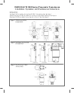
The TX AF circuits consist of microphone amplifier (MIC 
AMP) and AF fi lters. The AF fi lter cuts off the signals except 
voice signals (300 Hz or lower and 3 kHz or higher).

The audio signals from the internal microphone (MIC 
signals) are passed through MIC mute SW and amplifi ed by 
two MIC AMPs (#1 and #2). 

The MIC signals from the external microphone "EXMIC” are 
applied to the FRONT UNIT via [SP MIC] jack, and amplifi ed 
by MIC AMP (#2).

The amplified MIC signals "MIC” are applied to the MAIN 
UNIT via J401(FRONT UNIT) and J1 (MAIN UNIT).

The MIC signals from the FRONT UNIT are applied to the 
baseband IC (IC10, pin 3) and processed. 

SQUELCH CIRCUITS 

• NOISE SQUELCH

The noise squelch cuts off the AF output signals when 
no RF signals are received. Extracting noise components 
(approx. 30 kHz signals) in the demodulated AF signals, 
the squelch circuit turns the AF power amplifier and AF 
switches ON and OFF. 

A portion of FM-demodulated AF signal from the IF IC is 
adjusted its level (=squelch threshold level) by DAC (D/A 
converter; IC6, pins 1, 2), then passed through the noise 
filter (M: IC1, pins 7, 8 and R42, 44–46, C68–70) to extract 
the noise components (approx. 30 kHz signals) only. The 
noise components are rectified to be converted into the 
pulse-type signal by noise detector to produce DC voltage 
corresponding to the noise level "NOIS". Then the DC 
voltage is applied to the CPU (IC401, pin 41) and compared 
with the reference level preset in the CPU.

If the CPU interpretes that the noise level is higher than 
preset one, the CPU sets the "AFON" signal  to "High" to 
turn the  AF power AMP controller OFF, and the AF mute 
SW is turned OFF simultaneously. Thus closing the squelch 
is accomplished.
 

• TONE  SQUELCH

The tone squelch connects the RX AF line and activates 
the AF power amplifier to emit the AF signals only when 
receiving a signal which contains the tone frequency 
matched  with preset in the CPU. Detecting signal in the 
demodulated AF signals, the tone squelch circuit turns the 
AF power amplifier and AF switches ON and OFF. 

<CTCSS/DTCS>
A portion of FM-demodulated AF signals from the FM IF 
IC are passed through the tone filter (M: Q6, pins 5, 6) to 
remove unwanted voice siganls. The filtered tone signals 
are applied to the CPU (IC401, pin 44).

<2/5 TONE, DTMF>
A portion of FM-demodulated AF signals are output from 
the baseband IC (M: IC10, pin 21), and passed through 
the tone filter (M: R136, C220) to remove unwanted voice 
siganls. The filtered tone signals are applied to the CPU 
(IC401, pin 43).

The CPU compars the tone frequency/code preset in the 
CPU, and if the applied tone frequency/code is matched to 
preset one, the CPU controls the AF power AMP and AF 
mute SW as same as "NOISE SQUELCH." 

C512

R524

C405

R522

C437

C497

Q406

Q401, Q402

C510

R525

C513

R446

C404

W401

C421

R518

R407

R408

SP401

Q415

R511

R426

R519

R405

R513

W402

C496

C502

C481

C407

R401

R428

IC403

13

12

14

R539

C426

R520

C498

IC406

1

2

3

4

5 6 7 8

MC401

C503

C482

C435

R537

R433

R541

J402

1

2

3

4

5

6

C425

R523

C401

Q413

IC407

2

3

1

C406

R402

R445

R521

R538

R517

C423

R406

R430

R434

IC407

6

5

7

R432

R535

R512

R429

IC405

1

GND1 2

NC 3

OUT1 + 4

MODE 5

SVRR 6

SELECT 7

NC 8

OUT2 + 9

NC 10

GND2

11 VCC2

12 NC

13 OUT2-

14 IN2-

15 IN2+

16 IN1+

17 IN1-

18 OUT1-

19 NC

20 VCC1

SIGNAL

AFON

VCC

BEEP

DUSE

MIC

EXMIC

SPON

AFON

BPMAX

PWON

AFO

VR UNIT

W601

1

2

3

4

MIC/AF

MUTE SW

MIC AMP

#1

MIC AMP

#2

LPF

AF POWER AMP

CONTROLLER

AF POWER AMP

AUDIO
LEVEL

ADJUST

DAC

1

2

Noise
AMP

Fc=30 kHz

Active filter

From IF IC (Pin16)

To RX AF circuits

Noise detector

Rectify

“NOIS”

NOISE SQUELCH DIAGRAM

• TX  AF  CIRCUITS

Summary of Contents for IC-F50V

Page 1: ...VHF TRANSCEIVER S 14406XZ C1 Sep 2007...

Page 2: ...nited Kingdom Germany France Spain Russia and or other countries ORDERING PARTS 1 Make sure the problem is internal before disassembling the transceiver 2 DO NOT open the transceiver until the transce...

Page 3: ...CUITS 4 7 4 5 VOLTAGE BLOCK DIAGRAM 4 7 4 6 CPU F IC401 PORT ALLOCATIONS 4 8 SECTION 5 ADJUSTMENT PROCEDURES 5 1 PREPARATION 5 1 5 2 FREQUENCY ADJUSTMENT 5 4 5 3 TRANSMIT ADJUSTMENT 5 6 5 4 RECEIVE AD...

Page 4: ...oise without CCITT filter USA EXP CHN only 40 dB min 46 dB typ Wide 34 dB min 40 dB typ Narrow Residual modulation with CCITT filter EUR only 50 dB min 55 dB typ Wide 43 dB min 53 dB typ Middle 40 dB...

Page 5: ...IC12 CD4094BPWR MIC AMP IC407 NJM12904V AF BUFFER AF MIXER IC5 NJM12904V AF BUFFER IC6 NJM12904V TX POWER AMP Q7 RD07MVS2 T112 DRIVE AMP Q8 RD01MUS1 T113 LOCK VOLTAGE SWITCH IC17 TC4S66F BASE BAND IC...

Page 6: ...om the contact spring eUnsolder 1 point from the antenna connector Unsolder 6 shield cover Unsolder 4 contact spring Unsolder 1 antenna connector MAIN UNIT CHASSIS VR knob ANT nut Flat cable VR washer...

Page 7: ...gnals to the RX circuits is composed 1ST IF CIRCUITS The 1st IF circuits consist of 1st mixer 1st IF filter and 1st IF amplifier IF AMP And it converts the RX signals into the 1st IF signal then filte...

Page 8: ...M demodulated by the FM IF IC This transceiver employs the base band IC for audio signal processing for both transmit and receive The base band IC is an audio processor and composed of RF AMPlifier co...

Page 9: ...elch is accomplished TONE SQUELCH The tone squelch connects the RX AF line and activates the AF power amplifier to emit the AF signals only when receiving a signal which contains the tone frequency ma...

Page 10: ...C203 L37 R80 R85 C116 L28 R79 C139 C192 C119 D22 C123 R83 C134 C115 R78 Q13 R70 LVA RX VCO TX VCO R5V VCC T5V MOD BUFFER BUFFER BUFFER RIPPLE FILTER VCO SW TX RX SW Freq adjust Freq adjust Modulation...

Page 11: ...ortion to the transmit output power level The detected voltage is applied to the comparator The transmit power setting voltage is ap plied to another input terminal as the reference voltage The compar...

Page 12: ...D18 C156 D2 0 C133 C203 L37 R85 C116 L28 R79 C150 R187 C138 C154 C192 C119 D22 R108 R104 C123 R83 IC16 2 3 1 R117 C132 C134 C115 R9 1 R89 C208 C207 C145 C206 MB15A02PFV1 IC4 1 OSCIN 2 OSCOUT 3 VP 4 V...

Page 13: ...plied to the gate terminal of AGC line driver The driver controls the voltage which supplied to the RF AMP to control the gain of RF AMP C26 C186 R11 R12 R172 C42 6P C25 R15 R18 R13 D9 R22 C28 C22 R20...

Page 14: ...4 CDEC CTCSS DTCS signals I 45 VOXV VOX detect High start to transmit I 46 KR1 Key input for UP P0 and P3 keys Pulled up I 47 KR0 Key input for DOWN P1 and P2 keys Pulled up I 48 BATV Battery volatge...

Page 15: ...to 10 V Modulation Analyzer Frequency range 30 300 MHz Measuring range 0 to 10 kHz External speaker Input impedance 8 Capacity More than 1 W Audio generator Frequency range 300 3000 Hz Output level 1...

Page 16: ...he shortcut CS F50V on the desktop r Click Adjust Read button Clone Write I O Update F5 I O Check Adjust Read This screen is an example only Each transceiver has its own specific values for each setti...

Page 17: ...e here OPC 966U USB type Cloning cable GND MIC PTT GND GND SP PTT SWITCH AC MILLIVOLTMETER 10 mV to 10 V AUDIO GENERATOR 300 3000 Hz 1 500 mV SETTING Frequency 1 kHz Level 150 mV rms 4 7 F EXT SPEAKER...

Page 18: ...Power Meter to the antenna connector Transmitting 3 5 V CONVENIENT The PLL LOCK VOLTAGE can be adjusted automatically 1 Set the Lock voltage preset RX LVA and TX LVA to 179 2 Push the ENTER key on th...

Page 19: ...r to the antenna connector Transmitting Loosely couple a Frequency Counter to the antenna connector 174 000 MHz Loose Coupling FREQUENCY COUNTER 0 1 300 MHz RF POWER METER 10 W 50 5 2 FREQUENCY ADJUST...

Page 20: ...Transmitting Connect an RF power meter to the antenna connector 5 0 W Low2 L2 2 Channel 1 4 Transmitting 2 0 W Low1 L1 3 Channel 1 5 Transmitting 1 0 W 5 3 TRANSMIT ADJUSTMENT Select an adjustment ite...

Page 21: ...enna connector through an Attenuator 2 05 to 2 15 kHz Middle MOD Mid 2 Channel 1 7 Transmitting 3 15 to 3 25 kHz Wide MOD Wide 3 Channel 1 8 Transmitting 4 05 to 4 15 kHz EUR EUR 01 EUR 02 only 5 3 TR...

Page 22: ...n Analyzer Set to the square wave form Middle BAL Mid 2 Channel 1 10 Transmitting Wide BAL Wide 3 Channel 1 11 Transmitting EUR EUR 01 EUR 02 only 5 3 TRANSMIT ADJUSTMENT continued Select an adjustmen...

Page 23: ...nsmitting Connect a Modulation Analyzer to the antenna connector through an Attenuator 0 66 to 0 70 kHz 5 3 TRANSMIT ADJUSTMENT continued Select an adjustment item using keys then set to the specified...

Page 24: ...Put the cursor on the BPF T2 and push the return key CONVENIENT RECEIVE SENSITIVITY can be adjusted totally Put the cursor on the BPF ALL and push the return key 5 4 RECEIVE ADJUSTMENT Select an adjus...

Page 25: ...ceiving Push the return key to set the S6 level Automatic adjustment S METER S1 LEVEL 2 Set the SSG output level to 12 dB 119 dBm Receiving Push the return key to set the S1 level 5 4 RECEIVE ADJUSTME...

Page 26: ...elch Then set SQL value at the point where the audio signals just appear 5 4 RECEIVE ADJUSTMENT continued Select an adjustment item using keys then set to the specified value using keys on the connect...

Page 27: ...090 S RES ERJ2GEJ 104 X 100 k T 15 8 21 8 S Surface mount FRONT UNIT REF ORDER DESCRIPTION M H V NO NO LOCATION R484 7030005090 S RES ERJ2GEJ 104 X 100 k T 15 6 20 9 R485 7030005090 S RES ERJ2GEJ 104...

Page 28: ...960 S CER ECJ0EB1C183K T 6 3 23 4 C507 4030017730 S CER ECJ0EB1E471K T 5 23 C508 4030017730 S CER ECJ0EB1E471K T 11 3 24 2 C510 4550000460 S TAN TEESVA 1C 105M8R T 23 5 48 6 C512 4030018860 S CER ECJ0...

Page 29: ...E R10JFA T 58 8 4 8 L32 6200005721 S COL ELJRE 33NGFA T 37 1 32 1 L33 6200004480 S COL MLF1608D R82K T B 27 3 12 7 L35 6200003540 S COL MLF1608D R22K T B 27 8 18 1 L37 6200003640 S COL MLF1608E 100K T...

Page 30: ...J2GEJ 223 X 22 k C I F L only T 20 5 17 1 R208 7030010090 S RES ERJ2GEJ 180 X 18 C I F L only B 22 40 6 R210 7030005240 S RES ERJ2GEJ 473 X 47 k A G D J only B 18 7 41 3 R211 7030005240 S RES ERJ2GEJ...

Page 31: ...5 7 23 6 C225 4030017460 S CER ECJ0EB1E102K B 2 5 29 7 C227 4030016790 S CER ECJ0EB1C103K B 31 6 12 8 C228 4030017460 S CER ECJ0EB1E102K T 24 3 14 7 C229 4030016930 S CER ECJ0EB1A104K T 30 4 7 2 C230...

Page 32: ...O LOCATION EP3 6910015370 S BEA ACZ1005Y 102 T B 25 4 35 1 EP4 6910015600 S BEA ACZ1005Y 241 240 T 23 9 21 7 EP5 6910015600 S BEA ACZ1005Y 241 240 T 14 26 1 EP6 6910015370 S BEA ACZ1005Y 102 T B 28 8...

Page 33: ...50 2681 PTT PLATE 1 MP407 8930060711 2681 PTT RUBBER 1 1 MP408 8310059540 2681 LCD PLATE 1 MP409 8930060520 2681 LED LENS 1 MP410 8210019890 2681 REFLECTOR 1 MP411 8310069820 2681 WINDOW PLATE A 1 MP4...

Page 34: ...MP4 M MP408 F SP401 F DS401 F MP410 F R601 V MP424 F FRONT Unit MAIN Unit VR UNIT W601 V EP402 F MP429 F MP406 F MP421 F MP409 F MP407 F CONNECT UNIT J1 CO MP419 F W404 F W404 F A A MP406 F MP10 C MP1...

Page 35: ...500 R501 R502 R503 R506 R507 R508 R509 R511 R512 R513 R515 R516 R517 R518 R519 R520 R521 R522 R523 R524 R525 R526 R527 R528 R529 R530 R532 R533 R534 R535 R541 S401 X401 1 4 3 2 B6802B H0 H5 H10 H15 H2...

Page 36: ...321 C322 C323 C324 C325 C328 C329 D1 D2 D5 D12 D14 D15 D16 D17 D19 D20 D21 D22 D24 D26 EP3 EP6 EP8 FI1 FI2 FI2 IC1 IC4 IC7 IC18 IC19 L1 L2 L3 L4 L5 L6 L7 L8 L9 L11 L12 L13 L14 L15 L16 L17 L19 L20 L22...

Page 37: ...CTRL Q401 RSQ035P03TR Q402 KTC811U LCD DRIVE PRE Q9 2SC5110 LV ADJ D21 HVC375B LV ADJ D22 HVC375B MIC MUTE IC406 TC7W66FK AMP AMP HPF LPF LIMIT AMP LPF SCRM BLER BPF MSK DE Modu lator MSK Modu lator E...

Page 38: ...5 6 7 8 MA2S077 D404 150K R416 10K R475 0 015 C441 100K R472 KEY S404 KEY S406 47P C464 1K R486 0 001 C489 EM6027P MC401 100K R423 1 C503 CP10S CP5 0 001 C482 0 1 C412 27K R414 33 MSVB2 C435 10K R537...

Page 39: ...1 12K R121 0 001 C228 0 1 C180 0 001 C294 10K R161 0 1 C271 Q30 47K R129 100K R147 470 R120 0 001 C225 68K R151 0 001 C299 47P C250 0 01 C231 470 R196 R211 0 0022 C256 0 001 C230 KRC404E Q29 47K R132...

Page 40: ...C52 R33 150 ACZ1005Y EP6 0 1 C23 C43 0 001 Q11 2SC5107 C165 0 01 0 001 C159 C17 12P C167 0 1 C137 0 01 R52 150 CR 783 X2 1 VCON 2 GND 3 OUT 4 VCC Q2 3SK293 22P C205 R62 100 L19 47N 4 7 C211 R23 150K R...

Page 41: ...lenwood Centre 150 6165 Highway 17 Delta B C V4K 5B8 Canada Phone 1 604 952 4266 Fax 1 604 952 0090 URL http www icomcanada com E mail info icomcanada com Unit 1 103 Garden Road Clayton VIC 3168 Austr...

Page 42: ...1 1 32 Kamiminami Hirano ku Osaka 547 0003 Japan S 14406XZ C1 2007 Icom Inc...

Reviews: