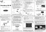
background image

5 - 1


SECTION 5. CIRCUIT 

DESCRIPTION

5-1 RECEIVER CIRCUITS

RF CIRCUITS (MAIN-A UNIT)

RF signal from the antenna is passed through the LPF (as 
the harmonic filter for transmitting) and antenna SW, and 
then applied to the RX BPF circuit.

The applied RX signal is passed through the 2-staged tuned 
BPF (D4, D8) to remove unwanted out-of-band signals, and 
amplified by the low-noise RF AMP (Q2), and then applied 
to the 1st mixer (Q3) through another 2-staged tuned BPF 
(D9, 10).

Total of 4 stage BPFs are tuned to the RX frequency by the 
tuning voltage “T1” and “T2” from the D/A converter (IC20), 
to obtain required IMD characteristic.

• RF CIRCUITS

1ST IF CIRCUITS (MAIN-A UNIT)

The RX signal from the BPF is mixed with the 1st LO signal 
to be converted into the 46.35 MHz 1st IF signal.

The 1st LO signal is generated by the RX VCO (Q14, D33, 
D34, L26, L39, etc.), and passed through the LO SW (D15) 
and attenuator, and then applied to the 1st mixer (Q3) 

The converted 1st IF signal is filtered by the crystal filter (FI1) 
and amplified by the 1st IF AMP (Q4), then applied to the IF 
demodulator IC (IC1).

• 1ST IF CIRCUITS

2ND IF AND DEMODULATOR CIRCUITS (MAIN-A UNIT)

The amplified 1st IF signal is mixed with the 2nd LO signal 
at the internal 2nd IF mixer of the IF demodulator IC (IC1), 
to obtain the 450 kHz 2nd IF signal.

The 15.3 MHz signal generated by the reference oscillator 
(X2) is passed through the filter AMP (Q34, L33, 35, C305–
308) to extract the 45.9 MHz 3rd harmonic component. 
The 45.9 MHz signal is then applied to the pin 2 of IF 
demodulator IC (IC1) as the 2nd LO signal. 

The converted 2nd IF signal is output from the pin 3 of IF 
demodulator IC (IC1), and filtered by the ceramic filters 
(FI2 and FI6 for Narrow mode; FI2 only for Wide mode) to 
remove unwanted out-of-band signals, and then applied to 
the internal frequency-demodulator of IF demodulator IC 
(IC1) from pin 5.

The demodulator is a quadrature type which uses X1 as the 
phase shifter.

The frequency-demodulated AF signal is output from pin 9 to 
AF circuits.

• 2ND IF AND DEMODULATORCIRCUITS

LPF

LP F

PWR
DET

D1,D11,D12

ANT

SW

D2,D3,D5,

D6,D47,D48

BPF

D9_B

BPF

D9_A

BPF

D4

BPF

D8

RF
AMP

Q2

AGC

Q1

Tuning voltage “T2”

To 1st IF circuits

Tuning voltage “T1”

136-174 MHz

RSSI

From the TX AMP

LO

SW

D15

Q3

1st mixer

BPF

XTAL

FI1

IF
AMP

Q4

LPF

From RF circuits

To IF IC

46.35 MHz

1st LO signals

(182.35 MHz-220.35 MHz)

REF

X2

X3

Q34

X1

BPF

BPF

CERAMIC

FI6

W/N

SW

Q5

BPF

CERAMIC

FI2

W/N

SW

D64,D65

Q40

W/N

SW

D66,D67

D/A

IF IC

From 1st IF circuits

IC1

IC18

AK2330

 NWC

15.3MHz

45.9MHz

DISC

SQIN

450kHz

To the AF circuits

NWC

Summary of Contents for iC-F5012

Page 1: ...S 14712XZ C1 Feb 2011 VHF MOBILE TRANSCEIVERS...

Page 2: ...ame and unit name 4 Quantity required ORDER EXAMPLE 1110007320 S IC NJM2591V IC F5012 MAIN UNIT 5 pieces 8820001210 Screw 2438 screw IC F5013 Top cover 10 pieces Addresses are provided on the inside b...

Page 3: ...CUITS 5 1 5 2 TRANSMITTER CIRCUITS 5 3 5 3 FREQUENCY SYNTHESIZER CIRCUITS 5 4 5 4 VOLTAGE DIAGRAM 5 4 5 5 PORT ALLOCATIONS 5 5 SECTION 6 ADJUSTMENT PROCEDURES 6 1 PREPARATION 6 1 6 2 FREQUENCY ADJUSTM...

Page 4: ...ver 1 1 kg 2 4 Ib TRANSMITTER Transmit output power 25 W ver 25 W High 10 W Low2 2 5 W Low1 50 W ver 50 W High 25 W Low2 5 0 W Low1 Modulation Variable reactance frequency modulation Max permissible d...

Page 5: ...65 dB typ Spurious response 70 dB min Intermodulation More than 70 dB 75 dB typ More than 65 dB 67 dB typ FM hum and noise Without CCITT filter Wide More than 40 dB 45 dB typ Narrow More than 34 dB 40...

Page 6: ...DE VIEWS TX RX INDICATOR LED DRIVERS Q13 and Q14 FRONT UNIT CPU IC1 RESET IC IC2 EEPROM IC3 TONE FILTER IC5 TONE FILTER SWITCH Q3 CLOCK FREQUENCY SHIFT DIODE D6 CPU CLOCK X1 KEY BACKLIGHT SW Q2 KEY BA...

Page 7: ...TOR IC IC1 TONE FILETR Q39 PLL IC IC4 CPU5 LINE REGULATOR IC10 RIPPLE FILTER Q17 VCO SWITCH Q15 VCC LINE SWITCH Q23 8V LINE REGULATOR IC9 R8 LINE REGULATOR Q30 APC AMP IC2 2ND IF FILTER BANDWIDTH SWIT...

Page 8: ...CE OSCILLATOR MODULATION BUFFER IC19 D A CONVERTER IC18 REFERENCE FREQUENCY OSCILLATOR X2 AF AMP IC15 EXPANDER IC17 AF LINE SW IC14 D A CONVERTER IC20 DRIVE AMP Q9 RF AMP Q2 1ST MIXER Q3 2ND IF FILTER...

Page 9: ...ews from the both sides and then remove the front panel in the direction of the arrow 4 Remove 9 screws from the PCB FLAT CABLE BOTTOM COVER SCREW 4 SCREW 2 FRONT PANEL SPEAKER CABLE UNSOLDER Solder r...

Page 10: ...tional product Otherwise no TX modulation or AF output is available Solder remover D 5 Short the pattern as below For modulation input Install optional UT 108R as follows 1 Turn OFF the power and then...

Page 11: ...e 2nd LO signal at the internal 2nd IF mixer of the IF demodulator IC IC1 to obtain the 450 kHz 2nd IF signal The 15 3 MHz signal generated by the reference oscillator X2 is passed through the filter...

Page 12: ...the D A converter IC18 and applied to the AF AMP IC15 through the AF line SW IC14 The amplified AF signal is applied to the AF power AMP IC8 and power amplified to obtain AF output level The power amp...

Page 13: ...tone signal modulation CTCSS 2 5 TONE MODULATION CIRCUIT MAIN A UNIT MIC signal from the splatter filter IC16 is level adjusted deviation adjustment by the D A converter IC18 and applied to the TX VCO...

Page 14: ...e difference is detected as a phase type signal and level adjusted at the charge pump then output The output pulse type signal is passed through the loop filter to be converted into the DC voltage Loc...

Page 15: ...89 CH2L Channel indicator LED for CH2 DS5 control High Lights O 90 CH1L Channel indicator LED for CH1 DS6 control High Lights O 95 LIGT2 Key backlight LED DS1 DS2 control High Backlight is ON O 96 TL...

Page 16: ...W or more Frequency Counter Frequency range Frequency accuracy Sensitivity 0 1 300 MHz 1 ppm or better 100 mV or better Standard Signal Generator SSG Frequency range Output level 0 1 300 MHz 0 1 V to...

Page 17: ...as below Select Middle NOTE FOR EUR versions when adjust Deviation Modulation Balance and S meter in the middle band change the bandwidth to Middle as below CONVENIENT The cloning data file for the ad...

Page 18: ...nsmit while SSG is connected to the antenna connector RF power meter 30 W 25 W ver 60 W 50 W ver DC power supply 13 6 V 20 A except EUR 13 2 V 20 A EUR Frequency counter Oscilloscope AC millivoltmeter...

Page 19: ...he adjustment value on the Adjust Utility screen RX LVA 1 1 V TX 2 Channel 1 2 Transmitting TX LVA 1 06 V RX 3 Channel 1 3 Receiving Click Update F5 button and then check the LVIN item on the I O Chec...

Page 20: ...r with an oscilloscope to the antenna connector through an attenuator and set it as HPF OFF LPF 20 kHz De emphasis OFF Detector P P 2 BAL No over or under shoot As flat as possible DEVIATION NARROW 1...

Page 21: ...ITIVITY MUST be adjusted before S METER When RECEIVE SENSITIVITY is re adjusted S METER MUST be re adjusted too 1 Channel 1 14 Receiving Connect an SSG to the antenna connec tor and set it as Frequenc...

Page 22: ...3 1790001241 S DIO MA2S7280GL T 31 8 39 7 D64 1750001910 S DIO HVD144AKRF E T 51 5 33 1 REF PARTS DESCRIPTION M H V NO NO LOCATION MAIN A UNIT M Mounted side T Mounted on the Top side B Mounted on the...

Page 23: ...0 R198 7030005050 S RES ERJ2GEJ 103 X 10K T 128 6 24 2 M Mounted side T Mounted on the Top side B Mounted on the Bottom side S Surface mount REF PARTS DESCRIPTION M H V NO NO LOCATION MAIN A UNIT R199...

Page 24: ...ESCRIPTION M H V NO NO LOCATION MAIN A UNIT C67 4030017460 S CER C1005 JB 1H 102K T B 60 4 23 2 C68 4030017430 S CER C1005 CH 1H 101J T T 52 1 25 2 C69 4030017430 S CER C1005 CH 1H 101J T T 53 9 25 2...

Page 25: ...05 CH 1H 070C T B 52 7 40 4 C342 4550000560 S TAN TEESVA 1V 334M8R T 78 4 66 1 C343 4030017460 S CER C1005 JB 1H 102K T B 51 5 39 1 C347 4030017460 S CER C1005 JB 1H 102K T T 52 1 24 3 M Mounted side...

Page 26: ...23 X 22K B 34 6 26 6 R26 7030005240 S RES ERJ2GEJ 473 X 47K B 32 9 24 8 R27 7030005240 S RES ERJ2GEJ 473 X 47K B 31 2 25 7 R28 7030005040 S RES ERJ2GEJ 472 X 4 7K B 34 6 23 9 R29 7030008290 S RES ERJ2...

Page 27: ...8 4030017460 S CER C1005 JB 1H 102K T B 8 9 17 4 C82 4030017420 S CER C1005 CH 1H 470J T B 36 3 23 0 C84 4030017420 S CER C1005 CH 1H 470J T B 25 5 27 5 C85 4030017420 S CER C1005 CH 1H 470J T B 32 9...

Page 28: ...1 1 REF ORDER DESCRIPTION QTY NO NO J1 6450002210 3017 8821 KIN 1 J2 6510027960 04 6294 040 000 800 1 J3 6510022022 14FLT SM2 TB LF SN M 1 SP1 2510001221 C052SB500 14 OSC 1 W1 8900010503 OPC 1046B 1 P...

Page 29: ...IT Unit abbreviations F FRONT UNIT M MAIN A UNIT C CHASSIS PARTS MP4 F MP3 F MP5 F MP11 F MP1 F SP1 F W1 C MP2 F MP9 F MP5 C 2 MP3 M IC3 M J1 C MP4 C MAIN A UNIT MP2 M MP2 C MP7 C 4 MP3 C 8 MP6 C J4 M...

Page 30: ...C385 C388 C394 C395 C396 C398 C401 C411 C436 C443 C451 C462 C463 C471 C472 C473 C474 C476 C477 C478 C479 C480 C481 C482 C484 C486 C487 C488 C489 C490 C492 CP1 CP28 D3 D3 D5 D5 D28 D37 D47 D48 D59 D61...

Page 31: ...Q13 Q14 Q25 Q25 Q27 Q27 Q28 Q28 Q29 Q29 Q31 Q34 Q34 Q35 Q35 Q36 Q36 R1 R4 R5 R6 R7 R8 R8 R9 R10 R11 R12 R13 R14 R15 R16 R17 R19 R20 R21 R22 R23 R26 R27 R28 R29 R30 R31 R36 R39 R40 R50 R54 R57 R67 R68...

Page 32: ...EE IC19 TA75S01F AMP X2 Q12 2SC5006 BPF HVD144A D54 55 TLV AD J D 53 HVC375B RLV AD J D 52 HVC375B W N SW D66 D67 HVD144A CP4 CP_3 CP_3 CP3 DS1 9 LNJ426W83RA DS10 CL 165 AMP IC21 TA75S01F BPF D9 B HVC...

Page 33: ...34 1 8K R135 1 5K R136 1 5K R137 1 5K R138 1 5K HR YG DS10 CL 165HR YG X1 CR 915 C30 10 R12 470 R139 1K C139 47P R130 390 R131 1 8K IC1 HD64F2238BTF13V 1 PE5 D5 2 PE6 D6 3 PE7 D7 4 PD0 D8 5 PD1 D9 6 P...

Page 34: ...R315 100K R314 100K R269 100K R270 100K R145 1K R143 1K R325 1K R326 1K R327 1K R144 1K R130 22K R135 270K R188 560 R187 10K R363 10K R362 100K R381 0 C315 0 022 C280 0 01 R159 10K J7 1 2 3 4 C267 0...

Page 35: ...C392 18P R48 C93 18P C401 R51 560K R54 10K R58 470 R59 18K R387 4 7K D18 HVL355CM L41 ELJRF Q12 2SC5006 L21 ELJRF L5 FHW1210HC L16 AS080547 47N C402 C403 C3 0 5P C5 0 5P C366 0 001 C6 22P R15 270K C9...

Page 36: ...454 7619 Glenwood Centre 150 6165 Highway 17 Delta B C V4K 5B8 Canada Phone 1 604 952 4266 Fax 1 604 952 0090 URL http www icomcanada com E mail info icomcanada com Unit 1 103 Garden Road Clayton VIC...

Page 37: ...1 1 32 Kamiminami Hirano ku Osaka 547 0003 Japan S 14712XZ C1 2011 Icom Inc...

Reviews: