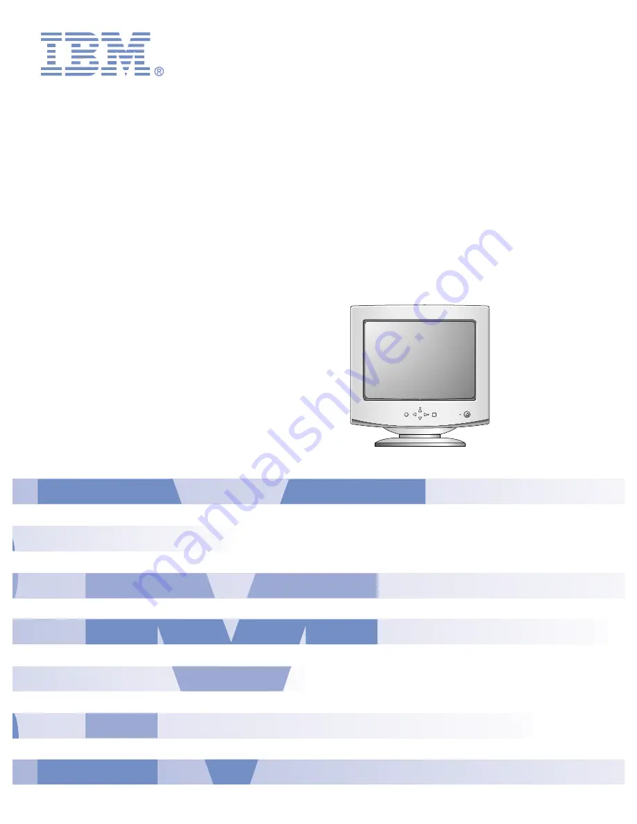
COLOR MONITORSERVICE MANUAL
CAUTION
BEFORE SERVICING THE UNIT, READ THE SAFETY PRECAUTIONS IN THIS MANUAL.
MODEL: E74
MENU
SELECT
CHASSIS NO. : CA-119
Page 1: ...COLOR MONITOR SERVICE MANUAL CAUTION BEFORE SERVICING THE UNIT READ THE SAFETY PRECAUTIONS IN THIS MANUAL MODEL E74 MENU SELECT CHASSIS NO CA 119 ...
Page 2: ...12 86 x 9 67 Preset Image Size 310 x 230 mm 12 20 x 9 06 4 2 Display Color Full Colors 4 3 Display Resolution 1280 x 1024 60Hz Max Non Interlace 4 4 Video Bandwidth 110 MHz 5 ENVIRONMENT 5 1 Operating Temperature 0 C 40 C Ambient 5 2 Relative Humidity 10 80 Non condensing 5 3 Altitude 3 000 m 6 DIMENSIONS with TILT SWIVEL Width 400 0 mm 15 74 inch Depth 420 0 mm 16 53 inch Height 395 0 mm 15 55 in...
Page 3: ...sign Soldering must be inspected for the cold solder joints frayed leads damaged insulation solder splashes or the sharp points Be sure to remove all foreign materials IMPLOSION PROTECTION All used display tubes are equipped with an integral implosion protection system but care should be taken to avoid damage and scratching during installation Use only same type display tubes X RADIATION The only ...
Page 4: ...6 20 282 6 085 2 028 3 042 1 014 V 85 039 11 759 10 546 1 213 0 079 1 107 0 026 H 43 27 23 112 17 778 5 334 1 556 2 222 1 556 V 85 01 11 763 11 093 0 670 0 069 0 578 0 023 H 41 775 23 938 18 238 5 7 2 052 3 42 0 228 V 75 13 333 12 663 0 670 0 551 0 096 0 024 H 60 02 16 66 13 00 3 66 1 22 2 24 0 20 V 75 03 13 328 12 795 0 533 0 050 0 466 0 017 Mode H V Sort 1 2 3 4 5 6 7 8 9 10 Dot Clock MHz Horizo...
Page 5: ...indicator lights up green when the monitor operates normally in DPMS Energy Saving mode stand by suspend or power off mode its color changes to orange and if abnormal or damaging circuit turns out orange blink 3 Select Button Use this button to enter a selection in the on screen display 4 Button Use these buttons to choose or adjust items in the on screen display 5 MENU Button Use this button to e...
Page 6: ...WIRING DIAGRAM 6 P501 P201 P405 P301 P302 G2 P702 P701 T1 P402 P902 S S Signal Cable AC Socket FBT ...
Page 7: ...rd 2 Pull the latch a carefully remove the Tilt Swivel by pulling it upward 3 Pressing the latch b Back cover by pushing it upward 4 Release the latch c 5 Slide the Back Cover away from the Front Cabinet of the monitor 2 TOTAL CHASSIS ASSEMBLY REMOVAL 1 Set the monitor face downward 2 Pressing the latch a Main Chassis by pushing it upward a a CDT Please be careful not to cut pattern ...
Page 8: ...2 H OUT Q706 H Linearity Correction DC DC Converter X RAY Protection Circuit FBT T701 Dynamic Focus Circuit Auto Beam Limit Vertical Blanking Brightness Control 160V 40V 400V STEP UP 13V D D Feed Back 13V MICOM IC401 SCL SDA H V Sync PWM Control 12V 5V 13V 105V 13V 10V 50V DY CDT Heater 6 3V I 2 C I 2 C I 2 C H V Sync G1 Screen G2 Dynamic Focus Static Focus H V R G B Drive Contrast Cut Off H DRV B...
Page 9: ...operating mode and offers the controlled data H size H position V size etc 4 The controlled data of each mode is stored in itself 5 User can adjust screen condition by each OSD function The data of the adjusted condition is stored in EEPROM IC402 6 Horizontal and Vertical Oscillation This circuit generates the horizontal pulse and the vertical pulse by taking the H and V sync signal This circuit c...
Page 10: ...e deflection yoke of the CRT 16 Video Pre Amp Circuit This circuit amplifies the analog video signal from 0 0 7V to 0 4V It is operated by taking the clamp R G B drive and contrast signal from the Micom IC401 17 Video Output Amp Circuit This circuit amplifies the video signal which comes from the video pre amp circuit and amplified it to applied the CRT cathode ...
Page 11: ...color data will be erased 4 Power button of the monitor turn off turn on 5 COMMAND PRESET START Y Yes command 6 DIST ADJ CTRL PWM TILT command 7 Adjust tilt as arrow keys to be the best condition 8 DIST ADJ BALANCE command 9 Adjust parallelogram as arrow keys to be the best condition 10 Adjust balance of pin balance as arrow keys to be the best condition 11 DIST ADJ FOS ADJ command 12 Adjust V SIZ...
Page 12: ...ay color 15 0 full white patten at Mode 10 21 COLOR ADJ LUMINANCE ABL command 22 Adjust ABL to 32 1FL of the luminance 23 After push the ENTER key and COMMAND PRESET EXIT Y Yes command 24 Exit from the program 5 Input EDID Data 1 Display color 15 0 cross hatch pattern at Mode 10 2 EEPROM Write EDID command and confirm EDID Write OK message of monitor 3 Exit from the alignment program 4 Power switc...
Page 13: ...E IN D900 TROUBLE IN FUSE F901 TROUBLE IN Q901 TROUBLE IN D941 D942 D951 D961 D971 TROUBLE IN Q903 Q952 Q951 Q942 Q941 CHECK FUSE OK CHECK C908 VOLTAGE AC120V 160VDC AC220V 304VDC NO YES YES YES YES NO NO NO CHECK Q901 PIN 6 WAVEFORM CHECK D941 D942 D951 D961 D971 VOLTAGE ...
Page 14: ...303 PIN 1 2 4 CHECK IC303 PIN 7 105V PIN 3 13V TROUBLE IN P302 5V LINE TROUBLE IN PC SIGNAL P301 SIGNAL CABLE TROUBLE IN IC302 TROUBLE IN P303 12V LINE 80V LINE TROUBLE IN IC303 NO YES NO NO YES YES YES YES NO NO CHECK R G B CATHODE VOLTAGE TROUBLE IN R331 R333 L311 L313 D307 D312 TROUBLE IN CRT SOCKET YES NO ...
Page 15: ...CHECK POWER INDICATOR GREEN or AMBER CHECK D712 ANODE 160V CHECK G1 VOLTAGE 55V 15V TROUBLE IN D712 TROUBLE IN Q799 DPM MODE NO H and or V SYNC AMBER NO GREEN YES NO CHECK CDT HEAT VOLTAGE 6 3V TROUBLE IN D941 Q942 Q941 YES NO TROUBLE IN CDT YES ...
Page 16: ...VERTICAL LINE CHECK Q706 CHECK B VOLTAGE 50V CHECK T701 FBT PIN 2 31KHZ 60V 69KHZ 140V CHECK Q705 COLLECTOR WAVEFORM TROUBLE IN Q706 TROUBLE IN 50V LINE TROUBLE IN Q719 Q703 Q704 D710 TROUBLE IN Q705 TROUBLE IN T701 P701 NO NO YES YES YES YES NO NO 0V T ...
Page 17: ...UBLE IN IC401 MICOM TROUBLE IN Q711 Q716 TROUBLE IN L703 TROUBLE IN C722 C723 C726 C729 NO NO NO YES YES YES Cs SIGNAL TABLE HORIZONTAL FREQUENCY fH 30K 33 9K 34K 38 9K 39K 43 9K 44K 48 9K 49K 51 9K 52K 57 9K 58K 61 9K 62K 65 9K 66K 70K Cs1 L L H H H H H H H Cs3 L L L H L L L H H Cs2 L H L L H H H H H ...
Page 18: ... 18 6 NO VERTICAL DEFLECTION NO V DEFLECTION ONE HORIZONTAL LINE CHECK IC601 PIN 2 13V CHECK IC701 PIN 23 TROUBLE IN D610 13V LINE TROUBLE IN IC701 TROUBLE IN IC601 V CIRCUIT NO YES YES NO 3V ...
Page 19: ...OUBLE IN IC601 PIN1 V FBP T701 40V LINE H FBP TROUBLE IN IC302 IC301 TROUBLE IN IC301 IC302 NO YES DC 5V YES YES YES NO NO NO Pin 5 5V Pin 10 5V H V 5V H V CHECK IC301 B 5V CHECK IC301 PIN 12 WAVEFORM ENTER BUTTON MUST BE PRESSED CHECK IC301 PIN 5 10 WAVEFORM CHECK IC301 PIN 13 14 15 ...
Page 20: ...V CHECK PC PC IS NOT GOING INTO DPM OFF MODE TROUBLE IN X401 TROUBLE IN IC401 MICOM TROUBLE IN Q941 Q942 Q951 Q952 TROUBLE IN PC OFF MODE FAILURE INPUT H V SYNC SIGNAL H V SYNC NO OFF MODE NO NO NO NO DPMF 0V DPM TABLE Mode Item NORMAL STAND BY SUSPEND OFF DPMF H L L L LED GREEN AMBER AMBER AMBER DPMS H H H L YES YES SEE DPM TABLE YES YES 5V 24MHz ...
Page 21: ...HECK Q953 COLLECTOR VOLTAGE CHECK P902 CHECK RL901 TROUBLE IN IC401 MICOM TROUBLE IN Q953 TROUBLE IN P902 TROUBLE IN RL901 TROUBLE IN TH901 DEGAUSSING COIL NO DEGAUSSING DC 15V NO NO NO NO YES YES YES YES DEGAUSS ON THE OSD MENU MUST BE PRESSED ...
Page 22: ...N NO TILT NO ROTATION TROUBLE IN IC401 MICOM TROUBLE IN 15V LINE 6 3V LINE TROUBLE IN Q501 Q503 TROUBLE IN P501 TILT COIL NO YES YES YES CHECK 13V LINE AND 6 3V LINE CHECK Q503 EMITTER VOLTAGE NO NO CHECK IC401 PIN21 WAVE FORM ...
Page 23: ...EXPLODED VIEW 8 B A 2 1 4 3 12 12 13 6 7 5 11 14 13 M E N U S E L E C T 10 9 a b c b 23 ...
Page 24: ...L TILT SWIVEL ASSEMBLY CB777G T053 B046 320T 9930 BK IBM SP LOCAL SCREW ASSY PHP 5 20 FZMY GW18 NEW TYPE COIL DEGAUSSING 1090MM 16 5OHM 0 4MM 110T 17 WITH EARTH FBT FLY BACK TRANSFORMER CF2077LG273A LIEN CHANGE 17 SOCKET CIRC POWER BAE EUN AC UNIVERSAL 3PIN BLACK SOCKET CIRC POWER SA 4S HUA JIE AC UNIVERSAL 3PIN BLACK CABLE D SUB UL20276 9C 5 8MM AT 1560MM BLACK 9930 TC170H DM PWB PCB ASSEMBLY SUB...
Page 25: ...PTION SPECIFICATION C706 0CE105CK638 1UF SHL SD 50V 20 FM5 TP 5 C708 0CE227CH638 220UF SHL SD 25V M FM5 TP 5 C709 0CE225CK638 2 2UF SHL SD 50V M FM5 TP 5 C710 181 288Q MKT 100V 154JTR PHS26154 C711 181 288E MKT 100V 474JTR PHS 26474 C712 181 288B MKT 100V 104JTR PHS26104 C713 0CK2210K515 220P 50V K B TS C714 0CE107CF638 100UF SHL SD 16V M FM5 TP 5 C715 181 288N MKT 100V 103JTR PHS86103 C717 0CE476...
Page 26: ...34 500MW D715 0DS141489AB 1N4148 TP GRANDE DO 34 500MW D716 0DR140059DA 1N4005TB52 TP LITEON DO41 60 DATE 2003 3 28 S AL LOC NO PART NO DESCRIPTION SPECIFICATION D717 0DR140059DA 1N4005TB52 TP LITEON DO41 60 D718 0DR140059DA 1N4005TB52 TP LITEON DO41 60 D719 0DR100009DA RGP10J TP GULF SEMICONDUCTOR D720 0DS141489AB 1N4148 TP GRANDE DO 34 500MW D721 0DS141489AB 1N4148 TP GRANDE DO 34 500MW D723 0DS...
Page 27: ...04 0RD4300Q609 430 OHM 1 4 W 3 4 5 00 TA5 R205 0RD1001Q609 1K 1 4W 3 5 TA52 R206 0RD0912Q609 91 OHM 1 4 W 3 4 5 TA52 R207 0RD4300Q609 430 OHM 1 4 W 3 4 5 00 TA5 R208 0RD2200Q609 220 1 4W 3 5 TA52 DATE 2003 3 28 S AL LOC NO PART NO DESCRIPTION SPECIFICATION R209 0RD9100Q609 910 1 4W 3 5 TA52 R210 0RD2200Q609 220 1 4W 3 5 TA52 R211 0RD2200Q609 220 1 4W 3 5 TA52 R301 0RD0752Q609 75 1 4W 3 5 TA52 R302...
Page 28: ... OHM 1 2 W 7 0 5 TA52 R741 0RD1000Q609 100 1 4W 3 5 TA52 R742 0RD3601Q609 3 60K 1 4W 3 5 TA52 DATE 2003 3 28 S AL LOC NO PART NO DESCRIPTION SPECIFICATION R743 0RD4701Q609 4 70K 1 4W 3 5 TA52 R744 0RD2700A609 270 OHM 1 2 W 7 0 5 TA52 R745 0RD4702Q609 47K 1 4W 3 5 TA52 R746 0RD2201Q609 2 20K 1 4W 3 5 TA52 R747 0RD3001Q609 3K 1 4W 3 5 TA52 R748 0RD4702Q609 47K 1 4W 3 5 TA52 R749 0RD2201Q609 2 20K 1 ...
Page 29: ...J86 0RD2400Q609 240 OHM 1 4 W 3 4 5 TA52 J302 0RD0471Q609 4 70 1 4W 3 5 TA52 RL901 6920TBA001A DY3MA DC12 DONGYANG 250VAC 1 SC301 6620TBD003A PCS701E PARK ELEC 10PIN 14 SC901 6620TKB002A BAE EUN AC UNIVERSAL 3PIN BL SG301 6918TAT005E MTAS 201M GIGA AXIAL TAPING SG302 6918TAT005E MTAS 201M GIGA AXIAL TAPING SG303 6918TAT005E MTAS 201M GIGA AXIAL TAPING SG305 6918TRT005A SSG 102 A0 1KV SMART RADIAL ...
Page 30: ...SYNC MONITORS 1 2 3 4 5 6 7 8 9 10 11 12 13 14 15 16 17 18 19 20 21 22 23 24 25 26 27 28 29 30 31 32 H HVSyn VSyn HLckVBk HPLL2C CO HGND RO HPLL1F HPosF HMoirØ HFly RefOut BComp BRegIn BISense HOscF HEHTIn VEHTIn VOscF VAGCCap VGND VCap VOut EWOut XRay HOut GND BOut Vcc SCL SDA VDyCor ...
Page 31: ...on asymm Parallelogram Hor duty cycle H moirØ am plitude VDyCor amplitude B ref Vertical size Vertical position Vertical moirØ Pin cushion Keystone Top corners Bottom corners Functions controlled via I 2 C Bus H size Control voltage level STV6888 Block Diagram ...
Page 32: ... 32 STV9211 Pin Configuration Pin Description ...
Page 33: ... 33 BLOCK DIAGRAM STV9211 ...
Page 34: ... 38 STV9556 1 2 3 4 5 6 7 8 9 10 11 OUT1 OUT2 OUT3 GNDP GNDA IN3 VDD GNDS VCC IN2 IN1 BLOCK DIAGRAM Pin Configuration ...
Page 35: ......
Page 36: ... 36 37 PRINTED CIRCUIT BOARD 3 MAIN BOARD Component Side 4 MAIN BOARD Solder Side 1 CONTROL BOARD Component Side 2 CONTROL BOARD Solder Side ...
Page 37: ...Apr 2003 Printed in Korea P NO 3828TSO056C ...