background image


SMARC2.0


RP-103-SMC 

Carrier Board for   

RM-N8/RM-N8M/RM-N8MMI   

CPU Module


User’s Manual 


September 2020 V.0.6 


Summary of Contents for RP-103-SMC

Page 1: ...SMARC2 0 RP 103 SMC Carrier Board for RM N8 RM N8M RM N8MMI CPU Module User s Manual September 2020 V 0 6 ...

Page 2: ...ability to use the product or the information contained herein nor for any infringements of rights of third parties which may result from its use Trademarks All the trademarks registrations and brands mentioned herein are used for identification purposes only and may be trademarks and or registered trademarks of their respective owners Acknowledgments NXP is a trademark of NXP Semiconductors N V I...

Page 3: ...gy and if not installed and used in accordance with manufacturer s instructions may cause harmful interference to radio communications WEEE This product must not be disposed of as normal household waste in accordance with the EU directive of for waste electrical and electronic equipment WEEE 2012 19 EU Instead it should be disposed of by returning it to a municipal recycling collection point Check...

Page 4: ...L BE BILLED FOR REPAIR AND SHIPPING CHARGES Technical Support Services 1 Visit the IBASE website at www ibase com tw to find the latest information about the product 2 If you need any further assistance from your distributor or sales representative prepare the following information of your product and elaborate upon the problem Product model name Product serial number Detailed description of the p...

Page 5: ... them Connect the device with 19 24V power input directly b To make a recovery SD card please refer to Chapter 3 c To use the root serial port debug function please check the section on COM1 debug cable setup information d To boot up with an installed LVDS panel please refer to Chapter 3 Note Different LVDS panel needs different customization please check with your sales contact e For advanced use...

Page 6: ... 3 Switch on RM N8MMI Q208I 14 2 4 Connectors on RP 103 SMC 15 2 5 Connector Functions on difference SMARC module 16 CN1 QSPI DF13E 10DP 1 25V 18 CN2 SPI3 DF13E 10DP 1 25V RM N8QM only 19 CN3 SPI0 DF13E 10DP 1 25V RM N8QM only 20 CN4 MIPI DSI0 21 CN5 Dual channel LVDS2 ch0 22 CN6 Dual channel LVDS2 ch1 23 CN7 DSI0 LVDS2 Backlight 24 CN8 DSI0 LVDS2 TP i2c for touch 25 CN9 MIPI DSI1 RM N8QM only 26 ...

Page 7: ... 47 CN32 FAN 48 CN33 UART 49 CN34 BTB Conn RM N8QM only 50 CN35 RTC BAT 52 P2 Internal DC in 53 P15 DSI0 LVDS2 Backlight Power Select 54 P16 DSI0 LVDS2 LCD Power Select 54 P17 DSI1 Backlight Power Select 55 P18 DSI1 LCD Power Select 55 P19 LVDS0 Backlight Power Select 56 P20 LVDS0 LCD Power Select 56 P21 LVDS1 Backlight Power Select 57 P22 LVDS1 LCD Power Select 57 P24 Line In Out 58 P26 RS232 422...

Page 8: ...al Chapter 3 Software Setup 63 Chapter 4 BSP Source Guide 65 4 1 1 Preparation 66 4 1 2 Installing Toolchain 66 4 1 3 Building release 67 4 1 4 Installing release to board 67 Chapter 5 Carrier Board Design Guide 69 Appendix 80 ...

Page 9: ...1 Chapter 1 Introduction The information provided in this chapter includes l IBASE i MX 8 Series SMARC Solution l SMARC Modules and RP 103 SMC Carrier Board l Board Dimensions l I O View l Installation ...

Page 10: ...ni processor Measuring 170mm x 170mm the RP 103 SMC VDDIO 3 3V carrier board is compatible with 82mm x 50mm standard SMARC form factors Engineers can choose the required embedded IOs to verify developed software application under specified operation systems aside from setting the default HDMI output with preloaded O S 1 2 SMARC Modules and RP 103 SMC Carrier Board Features of RM N8 QM408A l SMARC ...

Page 11: ...1x QSPI Media Interface 2x High speed MMC SDIO MMC 8 bit SDIO 4 bit PCIe 1x PCIe Gen 3 x 2 Lane 1x PCIe Gen 3 x 1 Lane GPIO 12x GPIO I C 4x I C CAN Bus 2x CAN Operating Temperature 25 C 85 C Board Connector MXM3 0 314 pins Operating System Supports Yocto v2 5 Android 9 This specification is subject to change without prior notice Features of RM N8M Q316I l SMARC Small Form Factor 82mm x 50mm SoM l ...

Page 12: ...ith OTG interface Image Capture Interface 2x MIPI CSI2 4 lane each Serial 4x UART 2x SPI Media Interface 2x High speed MMC SDIO MMC 8 bit SDIO 4 bit PCIe 2x PCI E x1 Gen2 GPIO 12x GPIO I C 4x I C CAN Bus N A Operating Temperature 25 C 85 C Board Connector MXM3 0 314 pins Operating System Supports Yocto v2 5 Android 9 This specification is subject to change without prior notice Features of RM N8MMI...

Page 13: ... H 264 Encoder Audio Interface 2x I2S 1x SPDIF LAN 1x RGMII USB 2x USB2 0 with OTG interface Image Capture Interface 1x MIPI CSI2 4 lane Serial 4x UART 2x SPI Media Interface 2x High speed MMC SDIO MMC 8 bit SDIO 4 bit PCIe 1x PCI E x1 Gen2 GPIO 12x GPIO I C 4x I C CAN Bus N A Operating Temperature 40 C 85 C Board Connector MXM3 0 314 pins Operating System Supports Yocto v2 5 Android 9 Features of...

Page 14: ...ual Channel LVDS two for RM N8 only 4x LCD backlight 2x MIPI CSI2 one for RM N8 RM N8M only 2x MIPI DSI one for RM N8 only 2x USB3 0 1x 12 GPIOs 2x RS232 RX TX only 2x I2C 2x SATA II and power one for RM N8 only 1x I2S 2x SPI for RM N8 only 1x QSPI 1x Full size Mini PCI E 1x SIM socket 1x M 2 Key E 2230 1x Speaker R and L 1 x RTC battery 2x UART for RM N8 only 1x 4 Wire UART Jumpers Switch Buttons...

Page 15: ...Introduction RP 103 SMC User Manual 7 1 ...

Page 16: ...8 RP 103 SMC User Manual 1 3 Board Dimensions RM N8 QM408A Dimensions RM N8M Q316I Dimensions RM N8MMI Q208I Dimensions ...

Page 17: ...Introduction RP 103 SMC User Manual 9 1 RP 103 SMC Dimensions ...

Page 18: ...10 RP 103 SMC User Manual 1 4 I O View ...

Page 19: ...MARC modules to the MXM slot on the board please perform the following steps Hold the SMARC module so that the edge fingers of the SMARC module aligns with the MXM connector Gently push the SMARC module to the MXM connector until the edge fingers of SMARC completely touch the bottom of the slot Gently press the SMARC module down and fix it with four screws ...

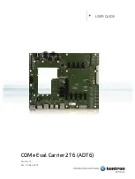
Page 20: ...12 Chapter 2 Jumpers and Connectors on the Carrier Board ...

Page 21: ... and switches on RP 103 SMC before doing the panel connection and boot up 2 1 Switch on RM N8 QM408A Mode Signal Name SW1_1 4 SW1_2 3 Normal Boot OFF OFF Auto Test OFF ON USB Download ON x 2 2 Switch on RM N8M Q316I Mode Signal Name SW1_1 4 SW1_2 3 Normal Boot OFF OFF Auto Test OFF ON USB Download ON x ...

Page 22: ...14 RP 103 SMC User Manual 2 3 Switch on RM N8MMI Q208I Mode Signal Name SW1_1 4 SW1_2 3 Normal Boot OFF OFF Auto Test OFF ON USB Download ON x ...

Page 23: ... 2 2 1 P16 DSI0 LVDS2 LCD power select CN16 LVDS1 Backlight 2 2 1 P17 DSI1 Backlight power select 2 2 1 CN17 LVDS1 TP i2c for touch 2 2 1 P18 DSI1 LCD power select 2 2 1 CN18 Speaker L P19 LVDS0 Backlight power select CN19 Speaker R P20 LVDS0 LCD power select CN20 USB3 4 P21 LVDS1 Backlight power select 2 2 1 CN21 MIPI CSI1 2 2 1 P22 LVDS1 LCD power select 2 2 1 CN22 MIPI CSI2 P23 Headphone Mic CN...

Page 24: ...DS2 LCD power select YES YES YES P17 DSI1 Backlight power select YES NO NO P18 DSI1 LCD power select YES NO NO P19 LVDS0 Backlight power select YES YES YES P20 LVDS0 LCD power select YES YES YES P21 LVDS1 Backlight power select YES NO NO P22 LVDS1 LCD power select YES NO NO P23 Headphone Mic YES YES YES P24 Line In Out YES YES YES P25 OTG USB YES YES YES P26 RS232 422 485 YES YES YES CN1 QSPI YES ...

Page 25: ...ES YES YES CN23 SATA0 YES NO NO CN24 SATA power YES NO NO CN25 SATA1 YES YES YES CN26 SATA power YES YES YES CN27 CAN0 1 YES NO NO CN28 CAN2 3 YES CAN2 CAN2 CN29 COM1 3 YES YES YES CN30 UART0 4 YES NO NO CN31 DIO YES YES YES CN32 FAN YES YES YES CN33 UART 4 wire YES YES YES CN34 BTB Conn YES NO NO CN35 RTC BAT YES YES YES SW1 Boot Mode Select YES YES YES SW2 UART Mode Select YES YES YES SW3 I O Di...

Page 26: ...18 RP 103 SMC User Manual CN1 QSPI DF13E 10DP 1 25V Pin Signal Name Pin Signal Name 1 1V8 2 QSPI_IO_3 3 QSPI_CS0_B 4 QSPI_SCLK 5 QSPI_CS1_B 6 QSPI_IO_0 7 QSPI_RST_B 8 QSPI_IO_1 9 QSPI_IO_2 10 GND ...

Page 27: ...on the Carrier Board RP 103 SMC User Manual 19 CN2 SPI3 DF13E 10DP 1 25V RM N8QM only Pin Signal Name Signal Name Pin 1 1V8 N C 2 3 SPI3_CS0_B SPI3_SCLK 4 5 SPI3_CS1_B SPI3_MOSI 6 7 N C SPI3_MISO 8 9 N C GND 10 ...

Page 28: ...20 RP 103 SMC User Manual CN3 SPI0 DF13E 10DP 1 25V RM N8QM only Pin Signal Name Pin Signal Name 1 1V8 2 N C 3 SPI0_CS0_B 4 SPI0_SCLK 5 SPI0_CS1_B 6 SPI0_MOSI 7 N C 8 SPI0_MISO 9 N C 10 GND ...

Page 29: ...nal Name Pin 2 MIPI_DSI0_CKN MIPI_DSI0_CKP 1 4 GND GND 3 6 MIPI_DSI0_DNO MIPI_DSI0_DP0 5 8 DSI0_VLCD GND 7 10 MIPI_DSI0_DN1 MIPI_DSI0_DP1 9 12 MIPI_DSI0_DN2 MIPI_DSI0_DP2 11 14 SPDIF_TX0 HDMI_INT 13 16 MIPI_DSI0_DN3 MIPI_DSI0_DP3 15 18 DSI0_VLCD LVDS0_TS_SCL 17 20 DSI0_BKLT LVDS0_TS_SDA 19 ...

Page 30: ...Signal Name 2 LVDS2_0_TX0_N 1 LVDS2_0_TX0_P 4 GND 3 GND 6 LVDS2_0_TX1_N 5 LVDS2_0_TX1_P 8 DSI0_VLCD 7 GND 10 LVDS2_0_TX3_N 9 LVDS2_0_TX3_P 12 LVDS2_0_TX2_N 11 LVDS2_0_TX2_P 14 GND 13 GND 16 LVDS2_0_CLK_N 15 LVDS2_0_CLK_P 18 DSI0_VLCD 17 DSI0_BL_PWM 20 DSI0_BKLT 19 DSI0_BKLT ...

Page 31: ...ignal Name Pin Signal Name 2 LVDS2_1_TX0_N 1 LVDS2_1_TX0_P 4 GND 3 GND 6 LVDS2_1_TX1_N 5 LVDS2_1_TX1_P 8 DSI0_VLCD 7 GND 10 LVDS2_1_TX3_N 9 LVDS2_1_TX3_P 12 LVDS2_1_TX2_N 11 LVDS2_1_TX2_P 14 GND 13 GND 16 LVDS2_1_CLK_N 15 LVDS2_1_CLK_P 18 DSI0_VLCD 17 DSI0_BL_PWM 20 DSI0_BKLT 19 DSI0_BKLT ...

Page 32: ...24 RP 103 SMC User Manual CN7 DSI0 LVDS2 Backlight Pin Signal Name 1 DSI0_BKLT 2 DSI0_BKLT_EN 3 DSI0_BKLT_PWM 4 GND ...

Page 33: ...Settings on the Carrier Board RP 103 SMC User Manual 25 CN8 DSI0 LVDS2 TP i2c for touch Pin Signal Name 1 1V8 2 TP_INT_B 3 TP_RST_B 4 LVDS0_TS_SCL 5 LVDS0_TS_SDA 6 GND ...

Page 34: ...ame 2 MIPI_DSI1_CKN 1 MIPI_DSI1_CKP 4 GND 3 GND 6 MIPI_DSI1_DNO 5 MIPI_DSI1_DP0 8 DSI0_VLCD 7 GND 10 MIPI_DSI0_DN1 9 MIPI_DSI1_DP1 12 MIPI_DSI0_DN2 11 MIPI_DSI1_DP2 14 SPDIF0_TX1 13 DSI1_INT_B 16 MIPI_DSI1_DN3 15 MIPI_DSI1_DP3 18 DSI1_VLCD 17 DSI1_TS_SCL 20 DSI1_BKLT 19 DSI1_TS_SDA ...

Page 35: ...Settings on the Carrier Board RP 103 SMC User Manual 27 CN10 DSI1 Backlight RM N8QM only Pin Signal Name 1 DSI0_BKLT 2 DSI0_BKLT_EN 3 DSI0_BKLT_PWM 4 GND ...

Page 36: ...gnal Name 2 LVDS0_0_TX0_N 1 LVDS0_0_TX0_P 4 GND 3 GND 6 LVDS0_0_TX1_N 5 LVDS0_0_TX1_P 8 LVDS0_VLCD 7 GND 10 LVDS0_0_TX3_N 9 LVDS0_0_TX3_P 12 LVDS0_0_TX2_N 11 LVDS0_0_TX2_P 14 GND 13 GND 16 LVDS0_0_CLK_N 15 LVDS0_0_CLK_P 18 LVDS0_VLCD 17 LVDS0_BL_PWM 20 LVDS0_BKLT 19 LVDS0_BKLT ...

Page 37: ...nal Name Pin Signal Name 2 LVDS0_1_TX0_N 1 LVDS0_1_TX0_P 4 GND 3 GND 6 LVDS0_1_TX1_N 5 LVDS0_1_TX1_P 8 LVDS0_VLCD 7 GND 10 LVDS0_1_TX3_N 9 LVDS0_1_TX3_P 12 LVDS0_1_TX2_N 11 LVDS0_1_TX2_P 14 GND 13 GND 16 LVDS0_1_CLK_N 15 LVDS0_1_CLK_P 18 LVDS0_VLCD 17 LVDS0_BL_PWM 20 LVDS0_BKLT 19 LVDS0_BKLT ...

Page 38: ...30 RP 103 SMC User Manual CN13 LVDS0 Backlight Pin Signal Name 1 LVDS0_BKLT 2 LVDS0_BKLT_EN 3 LVDS0_BKLT_PWM 4 GND ...

Page 39: ...Pin Signal Name Pin Signal Name 2 LVDS1_0_TX0_N 1 LVDS1_0_TX0_P 4 GND 3 GND 6 LVDS1_0_TX1_N 5 LVDS1_0_TX1_P 8 LVDS1_VLCD 7 GND 10 LVDS1_0_TX3_N 9 LVDS1_0_TX3_P 12 LVDS1_0_TX2_N 11 LVDS1_0_TX2_P 14 GND 13 GND 16 LVDS1_0_CLK_N 15 LVDS1_0_CLK_P 18 LVDS1_VLCD 17 LVDS1_BL_PWM 20 LVDS1_BKLT 19 LVDS1_BKLT ...

Page 40: ... Pin Signal Name 2 LVDS1_1_TX0_N 1 LVDS1_1_TX0_P 4 GND 3 GND 6 LVDS1_1_TX1_N 5 LVDS1_1_TX1_P 8 LVDS1_VLCD 7 GND 10 LVDS1_1_TX3_N 9 LVDS1_1_TX3_P 12 LVDS1_1_TX2_N 11 LVDS1_1_TX2_P 14 GND 13 GND 16 LVDS1_1_CLK_N 15 LVDS1_1_CLK_P 18 LVDS1_VLCD 17 LVDS1_BL_PWM 20 LVDS1_BKLT 19 LVDS1_BKLT ...

Page 41: ...Settings on the Carrier Board RP 103 SMC User Manual 33 CN16 LVDS1 Backlight RM N8QM only Pin Signal Name 1 LVDS1_BKLT 2 LVDS1_BKLT_EN 3 LVDS1_BKLT_PWM 4 GND ...

Page 42: ...34 RP 103 SMC User Manual CN17 LVDS1 TP i2c for touch RM N8QM only Pin Signal Name 1 1V8 2 LVDS1_TP_INT 3 LVDS1_TP_RST_B 4 LVDS1_TS_SCL 5 LVDS1_TS_SDA 6 GND ...

Page 43: ...Settings on the Carrier Board RP 103 SMC User Manual 35 CN18 Speaker L Pin Signal Name 1 SPK_LP 2 SPK_LN CN19 Speaker R Pin Signal Name 1 SPK_RP 2 SPK_RN ...

Page 44: ... User Manual CN20 USB3 4 Pin Signal Name Pin Signal Name 1 USB_PWR_OUT3 2 RXDM3 19 USB_PWR_OUT4 3 RXDP3 18 RXDM4 4 GND 17 RXDP4 5 TXDM3 16 GND 6 TXDP3 15 TXDM4 7 GND 14 TXDP4 8 DM3 13 GND 9 DP3 12 DM4 10 N C 11 DP4 ...

Page 45: ... Pin Signal Name Pin Signal Name 2 MIPI_CSI1_CKN 1 MIPI_CSI1_CKP 4 MIPI_CSI1_DNO 3 MIPI_CSI1_DP0 6 MIPI_CSI1_DN1 5 MIPI_CSI1_DP1 8 N C 7 N C 10 N C 9 N C 12 GND 11 GND 14 CSI1_SDA 13 CSI1_SCL 16 2V8 15 CSI1_RST_B 18 1V8 17 CSI1_PWEN_B 20 GND 19 CSI_MCLK Multi Pin are used with others ...

Page 46: ...SI2_CKN 1 MIPI_CSI2_CKP 4 MIPI_CSI2_DNO 3 MIPI_CSI2_DP0 6 MIPI_CSI2_DN1 5 MIPI_CSI2_DP1 8 MIPI_CSI2_DN2 7 MIPI_CSI2_DP2 10 MIPI_CSI2_DN3 9 MIPI_CSI2_DP3 12 GND 11 GND 14 CSI2_SDA 13 CSI2_SCL 16 2V8 15 CSI2_RST_B 18 1V8 17 CSI2_PWEN_B 20 GND 19 CSI_MCLK Multi Pin are used with others ...

Page 47: ...Settings on the Carrier Board RP 103 SMC User Manual 39 CN23 SATA0 RM N8QM only Pin Signal Name 1 GND 2 SATA0_TXP 3 SATA0_TXN 4 GND 5 SATA0_RXN 6 SATA0_RXP 7 GND ...

Page 48: ...40 RP 103 SMC User Manual CN24 SATA power RM N8QM only Pin Signal Name 1 5V 2 GND 3 GND 4 12V ...

Page 49: ...Settings on the Carrier Board RP 103 SMC User Manual 41 CN25 SATA1 Pin Signal Name 1 GND 2 SATA_TXP 3 SATA_TXN 4 GND 5 SATA_RXN 6 SATA_RXP 7 GND ...

Page 50: ...42 RP 103 SMC User Manual CN26 SATA power Pin Signal Name 1 5V 2 GND 3 GND 4 12V ...

Page 51: ...Settings on the Carrier Board RP 103 SMC User Manual 43 CN27 CAN0 1 RM N8QM only Pin Signal Name 1 CAN0_H 2 CAN0_L 3 GND 4 CAN1_H 5 CAN1_L 6 GND ...

Page 52: ...44 RP 103 SMC User Manual CN28 CAN2 3 Pin Signal Name 1 CAN2_H 2 CAN2_L 3 GND 4 CAN3_H 5 CAN3_L 6 GND ...

Page 53: ...Settings on the Carrier Board RP 103 SMC User Manual 45 CN29 COM1 3 Pin Signal Name 1 RS232_1_TX 2 RS232_1_RX 3 GND 4 RS232_3_TX 5 RS232_3_RX 6 GND ...

Page 54: ...46 RP 103 SMC User Manual CN30 UART0 UART4 RM N8QM only Pin Signal Name 1 UART4_TX 2 UART4_RX 3 GND 4 UART0_TX 5 UART0_RX 6 GND ...

Page 55: ...ignal Name 2 GPIO6 M2_I2C_IRQ_B 1 1V8 4 GPIO7 HP_DET_B 3 GPIO0 CSI1_PWEN_B 6 GPIO8 MIC_DET_B 5 GPIO1 CSI2_PWEN_B 8 GPIO9 TP_INT_B 7 GPIO2 CSI1_RST_B 10 GPIO10 TP_RST_B 9 GPIO3 CSI2_RST_B 12 GPIO11 M2_BT_DIS_B 11 GPIO4 HDA_RST_B 14 GND 13 GPIO5 M2_WIFI_DIS_B Multi Pin are used with others ...

Page 56: ...48 RP 103 SMC User Manual CN32 FAN Pin Signal Name 1 GND 2 12V 3 N C 4 N C ...

Page 57: ...Settings on the Carrier Board RP 103 SMC User Manual 49 CN33 UART Pin Signal Name 1 1V8 2 UART_TXD 3 UART_RXD 4 UART_RTS 5 UART_CTS 6 GND ...

Page 58: ... DSI1_DAT2 59 HDMI_RX_DAT2 10 DSI1_DAT2 60 HDMI_RX_DAT2 11 DSI1_DAT3 61 HDMI_RX_ARC 12 DSI1_DAT3 62 HDMI_RX_ARC 13 DSI1_BL_PWM 63 HDMI_RX_CEC 14 DSI1_TS_INT_B 64 HDMI_RX_SCL 15 DSI1_TS_SCL 65 HDMI_RX_SDA 16 DSI1_TS_SDA 66 HDMI_RX_MON 17 GND 67 HDMI_RX_HDP 18 LVDS1_CH0_CLK 68 M40_UART0_RX 19 LVDS1_CH0_CLK 69 M40_UART0_TX 20 GND 70 M41_UART4_RX 21 LVDS1_CH0_TX0 71 M41_UART4_TX 22 LVDS1_CH0_TX0 72 RS...

Page 59: ...1_TX0 84 SPI3_SDI 35 LVDS1_CH1_TX1 85 SPI3_CS0 36 LVDS1_CH1_TX1 86 SPI3_CS1 37 LVDS1_CH1_TX2 87 GND 38 LVDS1_CH1_TX2 88 SDHC1_CLK 39 LVDS1_CH1_TX3 89 SDHC1_CMD 40 LVDS1_CH1_TX3 90 SDHC1_DATA0 41 LVDS1_BL_PWM 91 SDHC1_DATA1 42 LVDS1_TS_INT 92 SDHC1_DATA2 43 LVDS1_I2C_SCL 93 SDHC1_DATA3 44 LVDS1_I2C_SDA 94 SDHC1_DATA4 45 LVDS1_TS_SCL 95 SDHC1_DATA5 46 LVDS1_TS_SDA 96 SDHC1_DATA6 47 GPT0_I2C_CLK 97 S...

Page 60: ...52 RP 103 SMC User Manual CN35 RTC BAT Pin Signal Name 1 LI_CELL 2 GND ...

Page 61: ...Settings on the Carrier Board RP 103 SMC User Manual 53 P2 Internal DC in Pin Signal Name 1 GND 2 GND 3 DC IN 4 DC IN ...

Page 62: ...SMC User Manual P15 DSI0 LVDS2 Backlight Power Select Mode Setting 3V3 1 2 ON 3 4 OFF 5 6 OFF 5V 1 2 OFF 3 4 ON 5 6 OFF 12V 1 2 OFF 3 4 OFF 5 6 ON P16 DSI0 LVDS2 LCD Power Select Mode Setting 3V3 1 2 ON 5V 2 3 ON ...

Page 63: ...rier Board RP 103 SMC User Manual 55 P17 DSI1 Backlight Power Select Mode Setting 3V3 1 2 ON 3 4 OFF 5 6 OFF 5V 1 2 OFF 3 4 ON 5 6 OFF 12V 1 2 OFF 3 4 OFF 5 6 ON P18 DSI1 LCD Power Select Mode Setting 3V3 1 2 ON 5V 2 3 ON ...

Page 64: ... 103 SMC User Manual P19 LVDS0 Backlight Power Select Mode Setting 3V3 1 2 ON 3 4 OFF 5 6 OFF 5V 1 2 OFF 3 4 ON 5 6 OFF 12V 1 2 OFF 3 4 OFF 5 6 ON P20 LVDS0 LCD Power Select Mode Setting 3V3 1 2 ON 5V 2 3 ON ...

Page 65: ...ier Board RP 103 SMC User Manual 57 P21 LVDS1 Backlight Power Select Mode Setting 3V3 1 2 ON 3 4 OFF 5 6 OFF 5V 1 2 OFF 3 4 ON 5 6 OFF 12V 1 2 OFF 3 4 OFF 5 6 ON P22 LVDS1 LCD Power Select Pin Setting 3V3 1 2 ON 5V 2 3 ON ...

Page 66: ...58 RP 103 SMC User Manual P24 Line In Out Pin Signal Name Pin Signal Name 1 N C 2 Analog_GND 3 LINE_IN_R 4 Analog_GND 5 LINE_IN_L 6 Analog_GND 7 Analog_GND 8 LINE_OUT_L 9 Analog_GND 10 LINE_OUT_R ...

Page 67: ...me 1 DCD Data carrier detect 6 DSR Data set ready 2 RXD Receive data 7 RTS Request to send 3 TXD Transmit data 8 CTS Clear to send 4 DTR Data terminal ready 9 N C 5 GND Pin RS 232 RS 422 RS 485 1 DCD TX DATA 2 RX TX DATA 3 TX RX NC 4 DTR RX NC 5 GND GND GND 6 DSR NC NC 7 TRT NC NC 8 CTS NC NC 9 NC NC NC ...

Page 68: ... Half Duplex 1T 1R RS 485 TX Enable Low Active OFF OFF OFF ON RS 485 Half Duplex 1T 1R RS 485 TX Enable High Active OFF ON ON OFF RS 422 Full Duplex 1T 1R RS 422 with termination resistor OFF OFF ON OFF Pure RS 232 1T 1R RS 232 co exists with RS485 OFF ON OFF OFF RS 485 Half Duplex 1T 1R RS 485 with termination resistor OFF OFF OFF OFF Low Power Shutdown All I O pins are High Impedance ON x x x x ...

Page 69: ...N OFF reserve OFF ON OFF OFF reserve ON OFF OFF OFF reserve OFF OFF OFF OFF Module eMMC Flash Default x x x ON Force Recovery SW1 Boot Mode Select for RM N8M RM N8MMI SW1 Function 1 8 2 7 3 6 4 5 ON ON OFF OFF reserve OFF ON OFF OFF reserve ON OFF OFF OFF reserve OFF OFF OFF OFF Module eMMC Flash Default x x x ON Force Recovery ...

Page 70: ... Select SW3_1 8 Function ON CN31 I O Free Definition OFF CN31 I O Normal Function Default DSI0 Output Select SW3 Function 2 7 3 6 ON ON DSI0 Output ON OFF LVDS2 Output OFF x LVDS0 CH0 Output DSI1 Output Select SW3_4 5 Function ON HDMI TX2 Output OFF DSI1 Output ...

Page 71: ...Software Setup RP 103 SMC User Manual 63 Chapter 3 Software Setup Make a Recovery SD card for advanced users only Display Parameter Setting in Kernel ...

Page 72: ...irection hmsupdate to SD card p1 root 2 Copy release files to hmsupdate imx boot imx8mqevk sd bin flash_evk fsl imx8mq evk dtb Image rootfs tar bz2 recovery tar bz2 3 Insert SD card in th board 4 Power up the board and the recovery program will start 5 When recovery is done power down the board and pull out the recovery SD card 3 2 Display Parameter Setting in Kernel SMARC2 0 supports HDMI output ...

Page 73: ...al 65 Chapter 4 BSP Source Guide This chapter is dedicated for advanced software engineers to build BSP source The topics covered in this chapter are as follows Preparation Installing Toolchain Building release Installing release to board ...

Page 74: ...stall libsdl1 2 dev xterm sed cvs subversion coreutils texi2html docbook utils python pysqlite2 help2man make gcc g desktop file utils libgl1 mesa dev libglu1 mesa dev mercurial autoconf automake groff curl lzop asciidoc i MX layers host packages for a Ubuntu 12 04 host setup only are sudo apt get install uboot mkimage i MX layers host packages for a Ubuntu 14 04 host setup only are sudo apt get i...

Page 75: ...d cd home bsp folder For Yocto Ubuntu Debian 1 cp file in release to windows 2 Set board to download mode and connect OTG to USB 3 Run uuu exe uuu auto or FW Download EMMC bat For Android 9 1 Copy the following file in out target product imx8mq 2 Set board to download mode and connect OTG to USB 3 run For 7GByte emmc uuu_imx_android_flash bat f imx8mq tos c 7 e or FW Download emmc 7GB bat For 16GB...

Page 76: ...68 RP 103 SMC User Manual This page is intentionally left blank ...

Page 77: ...sign Guide This Chapter is for advanced EE to create carrier boards or products Layout suggestions can also be found for RP 103 SMC carrier board design schematic file Please contact your sales representative in advance Block Diagram SMARC Module Interfaces Layout recommendations ...

Page 78: ...er Page 22 CN27 WTB 6pin Page 22 CAN0 MCP2562T ESN CAN1 I Os CN8 DSI Conn Page 10 CN6 DSI to LVDS Page 10 BL WTB 4pin Page 10 CN3 4 SN65DSI84TPAPRQ1 I2C CTP WTB 6pin LVDS Conn x2 CN5 MUX DSI0 LVDS0_CH0 TS3DV642A0RUAR LVDS0_CH1 BL WTB 4pin LVDS Conn DSI Conn CN14 15 CN9 Page 13 LVDS1_CH1 LVDS1_CH0 CN10 16 Page 14 HDMI Conn MIPI DSI1 HDMI RX P7 Page 11 Page 11 ADV7535BCBZ RL DSI to HDMI HDMI Conn P6...

Page 79: ... used as GPIO for other Carrier board P41 SD2_DATA2 SD I F Bidirectional 3 3V Can be used as GPIO for other Carrier board P42 SD2_DATA3 SD I F Bidirectional 3 3V Can be used as GPIO for other Carrier board P43 CSPI1_SS0 SPI I F Chip select Active Low Output High 1 8V Can be used as GPIO for other Carrier board P44 CSPI1_SCLK SPI I F Output 1 8V Can be used as GPIO for other Carrier board P45 CSPI1...

Page 80: ...ier board P75 M2_RST_B GPIO3_05 PCIe1 I F I O Module reset Active Low Output High 1 8V Can be used as GPIO for other Carrier board P76 NC P77 HDMI_AUXP HDMI I F P78 HDMI_AUXN HDMI I F P79 GND Ground P80 NC P81 NC P82 GND Ground P83 PCIe1_REFCKP PCIe1 I F P84 PCIe1_REFCKN PCIe1 I F P85 GND Ground P86 PCIe1_RX_P PCIe1 I F P87 PCIe1_RX_N PCIe1 I F P88 GND Ground P89 PCIe1_TX_P PCIe1 I F P90 PCIe1_TX_...

Page 81: ...V Can be used as GPIO for other Carrier board P118 TP_RST_B GPIO4_27 I O CapTouch panel Reset conrol Active Low Output Low 1 8V Can be used as GPIO for other Carrier board P119 TP_EN_B GPIO4_21 I O CapTouch panel control Active Low Output Low 1 8V Can be used as GPIO for other Carrier board P120 GND Ground P121 I2C4_SCL I2C I F Output 1 8V P122 I2C4_SDA I2C I F Bidirectional 1 8V P123 BOOT_SEL0 GP...

Page 82: ...IN System power 5V P153 VMAIN System power 5V P154 VMAIN System power 5V P155 VMAIN System power 5V P156 VMAIN System power 5V S1 I2C2_SCL I2C I F 1 8V S2 I2C2_SDA I2C I F 1 8V S3 GND Ground S4 NC S5 I2C1_SCL I2C I F 1 8V S6 CLKO1_CSI_MCLK MIPI CSI I F CSI MCLK Output 1 8V Can be used as GPIO for other Carrier board S7 I2C1_SDA I2C I F 1 8V S8 CSI_P1_CKP MIPI CSI1 I F Output S9 CSI_P1_CKN MIPI CSI...

Page 83: ...C3_SCL I2C I F Output 1 8V S49 I2C3_SDA I2C I F Bidirectional 1 8V S50 HDA_AUD2_TXFS I2S I F HAD Output 1 8V Can be used as GPIO for other Carrier board S51 HDA_AUD2_TXD I2S I F HAD Output 1 8V Can be used as GPIO for other Carrier board S52 HDA_AUD2_RXD I2S I F HAD Input 1 8V Can be used as GPIO for other Carrier board S53 HDA_AUD2_TXC I2S I F HAD Output 1 8V Can be used as GPIO for other Carrier...

Page 84: ...S79 NC S80 GND Ground S81 NC S82 NC S83 GND Ground S84 PCIe2_REFCKP PCIe2 I F S85 PCIe2_REFCKN PCIe2 I F S86 GND Ground S87 PCIe2_RX_P PCIe2 I F S88 PCIe2_RX_N PCIe2 I F S89 GND Ground S90 PCIe2_TX_P PCIe2 I F S91 PCIe2_TX_N PCIe2 I F S92 GND Ground S93 NC S94 NC S95 NC S96 NC S97 NC S98 NC S99 NC S100 NC S101 GND Ground S102 NC S103 NC S104 USB2_ID USB2 USB F Input High 1 8V S105 NC S106 NC S107 ...

Page 85: ...SI_CKP LVDS0 LVDS F S135 DSI_CKN LVDS0 LVDS F S136 GND Ground S137 DSI_DP3 LVDS0 LVDS F S138 DSI_DN3 LVDS0 LVDS F S139 I2C1_SCL I2C I F Output 1 8V S140 I2C1_SDA I2C I F Bidirectional 1 8V S141 LCD_BL_PWM PWMO1 LCD Backlight PWM Clock Output Low 1 8V Can be used as GPIO for other Carrier board S142 NC S143 GND Ground S144 NC S145 WDOG1_OUTPUT_B System watch dog reset output Active Low Output High ...

Page 86: ...DET_B GPIO4_20 I O PCBA autotest detect active Low Input High 1 8V Can be used as GPIO for other Carrier board S158 GND Ground 5 35 3 Layout Recommendations Signal impedance recommendation Signal Group Impedance Layout Tolerance All signals unless specified 50 Ω Single End 10 PCIE_TX RX Diff signals 85 Ω Differential 10 USB Diff signals 90 Ω Differential 10 Diff signals LVDS SATA HDMI DDR PCIE_CLK...

Page 87: ... 5 4 4 5 85 10 3 4 4 4 5 4 90 10 3 4 4 7 4 100 10 Layer Glass Style Cu Wt Thickness L1 0 5OZ plating to 1OZ 1 4 P P 3313 3 6 L2 0 5OZ 0 65 CORE 0 102 FR 4 4 L3 0 5OZ 0 65 P P 7628 7 1 CORE 0 71 FR 4 28 P P 7628 7 1 L4 0 5OZ 0 65 CORE 0 102 FR 4 4 L5 0 5OZ 0 65 P P 3313 3 6 L6 0 5OZ plating to 1OZ 1 4 Total thickness 62 8mil 1 595mm ...

Page 88: ... 1 How to Use GPIO in Linux Dsdsd 2 How to Use Watchdog in LinuxSdsd 3 eMMC Test 4 USB flash disk Test 5 SD Card Test 6 RS 232 Test 7 RS 485 Test 8 Audio Test 9 Ethernet Test 10 LVDS Test 11 HDMI Test 12 SATA hard disk Test 13 CAN Test ...

Page 89: ... example 2 Input echo 32 sys class gpio export echo in sys class gpio gpio40 direction cat sys class gpio gpio40 value 2 How to Use Watchdog in LinuxSdsd create fd int fd open watchdog device fd open dev watchdog O_WRONLY get watchdog support ioctl fd WDIOC_GETSUPPORT ident get watchdog status ioctl fd WDIOC_GETSTATUS status get watchdog timeout ioctl fd WDIOC_GETTIMEOUT timeout_val set watchdog t...

Page 90: ...e dd if dev urandom of tmp data1 bs 1024k count 10 write data to emmc dd if tmp data1 of MOUNT_POINT_STR data2 bs 1024k count 10 read data2 and compare with data1 cmp MOUNT_POINT_STR data2 tmp data1 eMMC speed test MOUNT_POINT_STR var get emmc write speed time dd if dev urandom of MOUNT_POINT_STR test bs 1024k count 10 clean caches echo 3 proc sys vm drop_caches get emmc read speed time dd if MOUN...

Page 91: ...flash being used Read write and check USB_DIR run media mmcblk1p1 create data file dd if dev urandom of var data1 bs 1024k count 100 write data to usb flash disk dd if var data1 of USB_DIR data2 bs 1024k count 100 read data2 and compare with data1 cmp USB_DIR data2 var data1 USB speed test USB_DIR run media mmcblk1p1 usb write speed dd if dev zero of BASIC_DIR i test bs 1M count 1000 oflag nocache...

Page 92: ...d the SD card Before starting the test make sure there is no critical data in the eMMC flash being used Read write and check SD_DIR run media mmcblk1 create data file dd if dev urandom of var data1 bs 1024k count 100 write data to SD card dd if var data1 of SD_DIR data2 bs 1024k count 100 read data2 and compare with data1 cmp SD_DIR data2 var data1 SD card speed test SD_DIR run media mmcblk1 SD wr...

Page 93: ... get_speed tcgetattr fd opt speed cfgetispeed opt set_parity options c_cflag options c_cflag CSIZE options c_cflag CSIZE options c_lflag ICANON ECHO ECHOE ISIG Input options c_oflag OPOST Output options c_cc options c_cc VTIME 150 options c_cc VMIN 0 set parity tcsetattr fd TCSANOW options write ttymxc1 write fd write_buf sizeof write_buf read ttymxc1 read fd read_buf sizeof read_buf ...

Page 94: ...speed tcgetattr fd opt speed cfgetispeed opt set_parity options c_cflag options c_cflag CSIZE options c_cflag CSIZE options c_lflag ICANON ECHO ECHOE ISIG Input options c_oflag OPOST Output options c_cc options c_cc VTIME 150 options c_cc VMIN 0 set parity tcsetattr fd TCSANOW options write ttymxc1 write fd write_buf sizeof write_buf read ttymxc1 read fd read_buf sizeof read_buf ...

Page 95: ... home root testscript ethernet lftp_library lib lftp server 192 168 1 123 lftp 192 168 1 123 EOF upload data to server 192 168 1 123 put data1 download data from server 192 168 1 123 get data1 exit lftp bye Ethernet Ping test ping server 192 168 1 123 ping c 20 192 168 1 123 tmp ethernet_ping txt Ethernet TCP test server 192 168 1 123 run command iperf3 s communicate with server 192 168 1 123 in t...

Page 96: ...ut the size of the screen in bytes screensize vinfo xres vinfo yres vinfo bits_per_pixel 8 Map the device to memory fbp char mmap 0 screensize PROT_READ PROT_WRITE MAP_SHARED framebuffer_fd 0 Figure out where in memory to put the pixel memset fbp 0x00 screensize draw point by fbp long int location 0 location x g_xoffset g_bits_per_pixel 8 y g_yoffset g_line_length fbp location 0 color_b fbp locati...

Page 97: ... yres vinfo bits_per_pixel 8 Map the device to memory fbp char mmap 0 screensize PROT_READ PROT_WRITE MAP_SHARED framebuffer_fd 0 Figure out where in memory to put the pixel memset fbp 0x00 screensize draw point by fbp long int location 0 location x g_xoffset g_bits_per_pixel 8 y g_yoffset g_line_length fbp location 0 color_b fbp location 1 color_g fbp location 2 color_r close framebuffer fd close...

Page 98: ...ed Reading writing test HD_DIR run media mmcblk1p1 create data file dd if dev urandom of var data1 bs 1024k count 100 write data to hard disk dd if var data1 of HD_DIR data2 bs 1024k count 100 read data2 and compare with data1 cmp HD_DIR data2 var data1 Hard disk speed test HD_DIR run media mmcblk1p1 hard disk write speed dd if dev zero of HD_DIR i test bs 1M count 1000 oflag nocache hard disk rea...

Page 99: ...ion set gpio to 1 echo 1 sys class gpio gpio106 value set gpio to 1 echo 0 sys class gpio gpio106 value config gpio to in mode echo in sys class gpio gpio106 direction get gpio value ret0_0 cat sys class gpio gpio106 value Testing CAN config can parrameter ip link set can0 type can bitrate 125000 triple sampling on enable can ifconfig can0 up disable ifconfig can0 down send data cangen can0 receiv...

Reviews: