background image

5

5

4

4

3

3

2

2

1

1

D

D

C

C

B

B

A

A

Servo MOTOR +5V

Servo 5V

PLL+3.3V

8202
kernel
+1.8V

Video
PLL
+1.8V

close to 8202

Debug Port

(PLL bypass)

Internal AD +3.3V

Video DAC +3.3V

3 mA

Audio PLL +3.3V

260mA

Video 5V

RF +3.3V

Flash +3.3V

SDRAM +3.3V

34ma~58ma(64Mx1)

5V

Flash +1.8V

8202S-16-SY-216-0-D

1.02

Power & Connnector

C

1

6

Monday, January 02, 2006

SUNPLUS TECHNOLOGY

Title

Size

Document Number

Rev

Date:

Sheet

of

OPTI_O

V_H_SYNC
V_V_SYNC

ASR

ASW

AFL

ASL

AFR

AC_C

COAX

B/U_O

AFR

AFL

R/V_O

G/Y_O

SIG_MODE

5

DIS_MODE

5

R/V_O

5

G/Y_O

5

B/U_O

5

V_H_SYNC

2

V_V_SYNC

2

V_H_SYNC

2

V_V_SYNC

2

MS_CLK

2

MS_D3

2

MS_D2

2

MS_D1

2

CARD_SENSE2

2

AFR

6

AFL

6

COAX

6

G/Y_O

5

R/V_O

5

B/U_O

5

AFL

6

AFR

6

CARD_WP

2

MS_BS

2

MS_D0

2

CARD_SENSE1

2

CARD_RST

2

GAME_CLK

2

GAME_LATCH 2

GAME_D1

2

GAME_D0

2

Y_O

5

Cr_O

5

CVB1_O

5

OPTI_O

6

CVB1_O

5

VFD_DATA

2

IR_IN

2

VFD_STB

2

VFD_CLK

2

ASL

6

AFR

6

AFL

6

ASW

6

AC_C

6

ASR

6

USB_DM

2

USB_DP

2

MIC_L

2

MIC_R

2

RFGND

A+5V

MGND

PLL3.3V

GND

GND

P+5V

M+5V

GND

VPLLVCC1.8

VGND

GND

V+5V

GND

GND

DVCC3

GND

GND

GND

GND

GND

GND

P+5V

RFGND

USB_PLL3.3

VVCC3

APLLVCC3

SD_VCC3

ROM_VCC3

VCC1.8

VGND

VGND

DVCC

GND

GND

GND

VGND

GND

OPTI_VDD

VGND

GND

P+12V

GND

P-12V

USB+5V

P+5V

GND

GND

P+5V

P+5V

DVCC3

VGND

VGND

DVCC

VGND

P+12V

AVCC12

AGND

GND

P-12V

AVCC-12

AGND

GND

AGND

GND

AGND

GND

AD_GND

VCC3A

AD_GND

MGND

RFGND

AGND

GND

DVCC3

GND

MGND

GND

DVCC

VGND

+5AVAA

RF3.3V

RFGND

RFGND

GND

VGND

GND

GND

GND

USB+5V

GND

GND

GND

P+12V

AD_GND

VGND

GND

ROM_VCC1.8

GND

C72

NC

BC5

0.1UF

+

EC13
100UF16V

C61

33PF

CN1

POWER

1
2
3
4
5
6

R69

33

BC16

0.1UF

L28

FB

L34

FB

R114
15K

R119

22

R37

220

R59
4.7K

CN7

SCART

1
2
3
4
5
6
7
8
9
10
11
12
13

L2

FB

CN11

Card board power

1
2

L20

FB

R36
470

AV1

OPTI OUT

5

4

6

7

8

2

3

1

GND

VCC

OUT

NC

NC

NC

NC

NC

L31

FB

R34
470

TP18

L8

FB

+

EC14
100UF16V

R35

750

+

EC24

100UF16V

C63

33PF

R67
4.7K

R113

22

TP16

BC29

0.1UF

R48
220

L14

FB

L24

FB

AV2

comp/S-video

1

2

3
4

5

6

7
8

9
10

1

2

3
4

5

6

7
8

9

10

L23

FB

+

EC17
100UF16V

+

EC5

100UF16V

EC4

470UF16V

+

EC43

220UF16V

L25

FB

+

EC29

100UF16V

D1

1N4004

R56
220

R2

2.2

AV4

AV-JACK-1

1

3

2

6

5

4

9

8

7

1

3

2

6

5

4

9

8

7

TP23

BC8

0.1UF

BC12

0.1UF

BC64

0.1UF

L26

FB

CN10

HEADER4-2.54

1
2
3
4

BC65

0.1UF

BC39

0.1UF

EC2

220UF16V

+

EC10

220UF16V

C55

33PF

R46
4.7K

C69

NC

TP15

L22

FB

L27

FB

C49

33PF

U3

AMS 1085 TO-252

1

3

2

ADJ

IN

OUT

L3

FB

L30

FB

CN6

UART debug

1
2
3
4

+

EC15

100UF16V

L33

FB

BC20

0.1UF

EC47

220UF16V

BC41

0.1UF

R82

2.2

Q12

2N3906

R51
4.7K

L7

NC

CN9

IR/VFD

1
2
3
4
5
6

BC13

330PF

+

EC3
100UF16V

+

EC16

100UF16V

L1

FB

L19

FB

L21

FB

BC36

100PF

L29

FB

CN5

GAME

1
2
3
4
5
6

AV3

AV-JACK-1

1

3

2

6

5

4

9

8

7

1

3

2

6

5

4

9

8

7

R111

33

Q13

2N3906

BC11

33PF

+

EC42

100UF16V

BC25

0.1UF

RN1
1K(8 Pin, 4R)

1

3

5

7

8

6

4

2

BC15

0.1UF

BC27

0.1UF

+

EC25

100UF16V

TP19

L5

FB

CN12

MIC

1
2
3
4

U2

AMS1085 TO-252

1

3

2

ADJ

IN

OUT

F1

FUSE(1206,500mA)

1

2

L10

FB

+

EC1
100UF16V

CN8

CARD

1
2
3
4
5
6
7
8
9

10
11
12
13
14
15
16

BC9

0.1UF

R66

33

BC26

0.1UF

R117
15K

R115

10

BC40

0.1UF

BC2

0.1UF

Summary of Contents for H-MS1107

Page 1: ...Service Manual H MS1107 rev 1 01 Include 2006 09 29 HYUNDAI Electronics Service Support Team RUS...

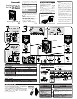
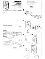
Page 2: ...Page 1 SERVICE MANUAL DVD PLAYER For Sunplus...

Page 3: ...Page 2 Contents Front cover 01 01 Contents 02 02 Block diagrams for the DVD player 03 08 Major functions of the IC of the DVD player 15 15 Maintenance procedures for the DVD player 16 23...

Page 4: ...cuit Digital servo processor Control decoding single chip microcomputer SPHE8200A control Feeding motor Focusing coil Trace searching coil Principal axis motor Disc tray ingress and egress controller...

Page 5: ...or the power supply part of the DVD player Faceplate power supply 12V 12V 5V 3 3V 220V Switch transformer Switch tube control Filter by the filter capacitor after diode rectification Power switch cont...

Page 6: ...Block diagram for the faceplate part of the DVD player Signals DATA STB and BCK of decoding board output VFD display drive Matrix circuit button VFD screen Faceplate button AC 3 3V 5V 21V from power...

Page 7: ...Page 6 Block diagram for the karaoke part of the DVD player Microphone input Preamplifier 4558 AF amplifier VOLUME CONTROL OF THE MICROPHONE Two channel output AF signal...

Page 8: ...racking control Laser tube Gliding mechanism of the light head Focusing servo makes the focus match the information side of a CD Tracking servo makes the light beam track the sound track Feeding servo...

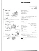
Page 9: ...Page 8 Major functions of the IC feet ED86 interface figure...

Page 10: ...processor central processing MPEG decoding VF coder 3 5954 function drive chip 4 CS4360 audio D A converter 5 KM16x256K function random dynamic processor 6 29F040A function flash memory FLASH Other I...

Page 11: ...h transformer to find out if it is normal or not Check the power board part The transformer is broken YES NO YES YES YES NO YES NO NO NO YES NO No reaction when the machine is turned on then check if...

Page 12: ...if the output standard voltage of the switch transformer is normal or not Maintain using the maintenance method adopted for the power supply card Insert the power terminal in place Check if the rectif...

Page 13: ...t is correctly set or not Use the oscilloscope to test if the AF signal at the O A output end is normal or not YES Check if the waveforms of the five data LRCK DATA1 DATA2 DATA3 and BCK of the decodin...

Page 14: ...normal or not If there is no voltage then check the power supply part Check if the 27MHz crystal oscillator on the decoding board is oscillating see the attached figure 6 Replace it with a crystal osc...

Page 15: ...ce it with a laser head of the same model Replace it with an IC of the same model NO NO NO NO YES YES Check if the contact of the 24P light head terminal is normal or not Replace it with a terminal of...

Page 16: ...re not YES NO Replace the VFD display screen Check if there is any voltage output at the power supply feet Replace the 16312 if a fault is found NO YES YES Replace the buttons Test if the three data l...

Page 17: ...ine between the volume potentiometer and the operational amplifier IC is normal or not Check if the operational amplification circuit and the reverberation IC are working normally or not Replace the M...

Page 18: ......

Page 19: ......

Page 20: ...D 5AVAA RF3 3V RFGND RFGND GND VGND GND GND GND USB 5V GND GND GND P 12V AD_GND VGND GND ROM_VCC1 8 GND C72 NC BC5 0 1UF EC13 100UF16V C61 33PF CN1 POWER 1 2 3 4 5 6 R69 33 BC16 0 1UF L28 FB L34 FB R1...

Page 21: ...P1 RAD R49 4 7K BC50 0 1UF C62 TP12 DFCT C28 TP25 GPIO BC46 0 1UF R58 0 C26 0 1UF R97 5 1K EC9 47UF16V R52 NC R44 C87 0 1UF EC8 47UF16V C99 0 47UF R243 330 R174 NC R47 4 7K BC45 0 1UF C65 33PF R96 L11...

Page 22: ...1 53 36 20 1 27 28 41 22 40 3 9 43 49 6 12 46 52 35 21 54 14 A0 A1 A2 A3 A4 A5 A6 A7 A8 A9 CAS RAS LDQM WE CS CKE CLK UDQM D0 D1 D2 D3 D4 D5 D6 D7 D8 D9 D10 D11 D12 D13 D14 D15 NC BA0 VDD VDD VSS VSS...

Page 23: ...RAD 2 TRAYOUT 2 TRAYIN 2 HOME 2 M 5V MGND M 5V MGND MGND MGND MGND MGND M 5V 0 R12 C16 4700PF NC R202 NC R6 CN3 JST CON6 2 mm 1 2 3 4 5 6 NC R18 R33 470K NC R248 0 R4 NC R8 0 R203 0 R19 R27 150K NC C...

Page 24: ..._O SY SCART_SIG DISPLAY_MODE RELEASE_SCART Y_O 1 CVB1_O 1 G Y_O 1 R V_O 1 B U_O 1 SCART_SIG 2 SCART_DISPLAY 2 SIG_MODE 1 DIS_MODE 1 V_BIAS 2 V_REF 2 V_FSADJ 2 TV_DAC3 2 TV_DAC4 2 V_COMP 2 TV_DAC0 2 TV...

Page 25: ...3 2 1 8 4 EC23 10UF16V EC33 10UF16V R130 10K C60 47PF R126 0 EC19 10UF16V C59 100PF Q28 2N3906 2 1 3 EC21 10UF16V BC43 0 1UF U9 CS4334 1 2 3 4 5 6 7 8 SDATA DEM SCLK LRCK MCLK AOUTR AGND VA AOUTL R12...

Reviews: