Hoft & Wessel HW 86010 Integration Manual Download Page 13

HW 86010

Integration Manual

© Höft & Wessel AG

1

4

<

!

Subject to amendment, errors excepted

IM86010-1-22_.doc

1.22

30.07.04

AM

page 13/46

Figure 5:

Recommended mounting of external antenna

An external antenna (50

 impedance) may be connected as indicated.
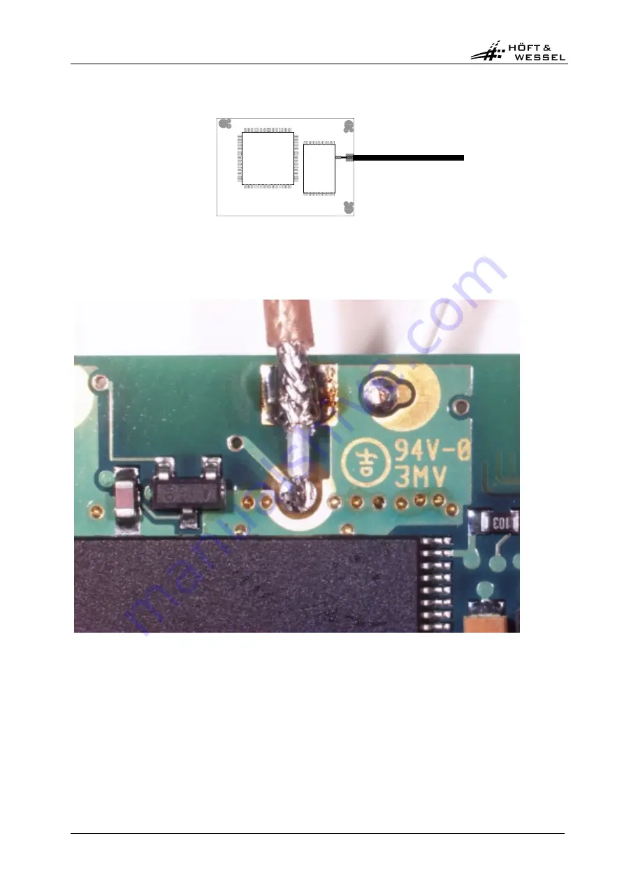
Figure 6:

Soldering the external antenna

Summary of Contents for HW 86010

Page 1: ...HW 86010 DECT Transceiver Module Integration Manual Version 1 22 ...

Page 2: ......

Page 3: ...t Integration Manual Version 1 22 Date of issue 16 01 2002 Authors Dr Andreas Müller Höft Wessel AG Change history 0 20 14 01 00 First pre release version 0 80 Internal release 0 90 05 05 00 For comments missing protocol mode 1 00 First official release 1 19 take out firmware description internal release 1 20 External release 1 21 Added picture on antenna soldering 1 22 Corrections ...

Page 4: ...mbly 12 3 2 Electrical characteristics 14 3 2 1 Supply voltage V3P3 14 3 2 2 Supply voltage VBATP 15 3 2 3 Logical signals 16 3 3 Radio specification 17 3 4 Interface description 18 3 4 1 Connector specification 18 3 4 2 Connector pinout 19 3 4 3 RS 232 interface 20 3 4 4 Voice Interface 21 3 4 5 ADC PWM interface 24 3 4 6 Reset Interface 25 3 4 7 I C Interface 30 3 4 8 PCM Interface 33 3 4 9 Gene...

Page 5: ...o not hesitate to contact us Your feedback will enable our specialists to solve your problems and continually improve our products and documentation 1 1 About this document This integration manual contains the full technical specification of the HW 86010 as well as all necessary information for a successful integration HW 86010 is a future proof product which offers a number of flexible interfaces...

Page 6: ...32829 Telefax 49 511 6102 411 Email info hoeft wessel de If you have general questions concerning Höft Wessel communication products you may directly contact the communications department Telephone 49 511 6102 333 Telefax 49 511 6102 437 Email eko hoeft wessel de Latest revisions of all publicly available documentation and firmware downloads are available from our web site www hoeft wessel de Höft...

Page 7: ...tems I C for auxiliary functions and analogue input output for voice Additional general purpose I Os plus an accessible bus interface make the HW 86010 ideally suited for automation and control applications with specific I O requirements The RF section of the HW 86010 comprises a single blind slot radio fully compliant with EN 300 175 2 It offers improved functionality Three antenna connections al...

Page 8: ...ed for control of on board peripherals half duplex GPIO General purpose digital I O pins DECT core Dedicated µC that runs the DECT firmware Radio RF section that generates and receives radio signals Bus Direct interface to the internal bus of the core µC FLASH Non volatile memory used to store the firmware and parameters Voice Interfaces for microphone speaker and ringer ADC PWM Analogue input and...

Page 9: ...ment errors excepted IM86010 1 22_ doc 1 22 30 07 04 AM page 9 46 2 3 Environmental Conditions 2 3 1 Storage Temperature Range C Nominal 25 to 75 2 3 2 Operating Temperature Range C Nominal 15 to 35 Extreme 10 to 55 2 3 3 Humidity rel Nominal 0 to 90 non condensing ...

Page 10: ...M86010 1 22_ doc Subject to amendment errors excepted 3 0 Hardware description 3 1 Mechanical characteristics 3 1 1 Dimensions mm Length 53 0 tolerances see section 3 1 3 Width 37 0 tolerances see section 3 1 3 Height 7 2 tolerances see section 3 1 3 3 1 2 Weight g Weight 18 2 ...

Page 11: ...HW 86010 Integration Manual Höft Wessel AG 1 4 Subject to amendment errors excepted IM86010 1 22_ doc 1 22 30 07 04 AM page 11 46 3 1 3 Mechanical drawing Figure 2 Mechanical drawing ...

Page 12: ...n of internal wire antenna 37 00 mm 5 00 mm 1 00 mm 45 00 mm Silver plated copper wire 0 75 mm 90 Shrink on sleeve Figure 3 Internal wire antenna 3 1 4 2 Mounting of antennas 80 90 Figure 4 Recommended mountings of internal wire antennas Caution Be careful not to shortcut or ground the antennas since this may damage the HW 86010 The antennas are DC coupled with the module ...

Page 13: ...G 1 4 Subject to amendment errors excepted IM86010 1 22_ doc 1 22 30 07 04 AM page 13 46 Figure 5 Recommended mounting of external antenna An external antenna 50Ω impedance may be connected as indicated Figure 6 Soldering the external antenna ...

Page 14: ...t is the reference voltage for all digital I Os The current consumption on V3P3 depends on the power management Power management only applies to the PT not to the FT The PT may enter a sleep mode whilst the FT is always active During firmware download the current consumption is higher because additional power is needed for writing the Flash memory Mode average I3P3 peak I3P3 Sleep mode PT only 9mA...

Page 15: ...mA 300mA Idle mode FT only 50mA 400mA 1 traffic bearer 50mA 400mA 4 traffic bearers 110mA 400mA All values are approximate figures measured under typical operating conditions IBATP 100mA div t 2ms div Figure 7 Typical IBATP bursts multi bearer connection active The current consumption on VBATP depends on the power management and on the number of active traffic bearers Power management only applies...

Page 16: ... finds a suitable FT In scan mode the PT requires more power Caution When a PT does not receive a valid FT it enters scan mode This may reduce stand by time of battery powered devices Try to avoid this situation 3 2 3 Logical signals Signal min max Logical high output V3P3 0 3V V3P3 Logical low output 0 0V 0 5V Logical high input 0 7 x V3P3 V3P3 0 3V Logical low input 0 5V 0 3 x V3P3 Iout output l...

Page 17: ... slot duplex bearers Number of bearers used at the same time 6 Total system data rate 7 5 Mbit s at the air interface Maximum data rate for a single radio 384 kbit s at the air interface Data rate per bearer per direction 32 kbit s at the air interface Transmitter power 250mW during active transmit slot Range inhouse up to 50m outdoor up to 300m Reference timer accuracy better than 5 ppm at nomina...

Page 18: ...W 86010 is bottom entry i e through the printed circuit board A suited connector is Samtec FTSH 125 01 The following figures illustrate two preferred mounting scenarios 2 0 mm Connector Connector Figure 8 No components fitted on target PCB below HW 86010 Minimum distance between PCBs 2 0 mm When Samtec FTSH 125 01 is used as mating connector minimum distance between the PCBs is 2 92mm as given by ...

Page 19: ...O GPIO6 18 17 GPIO5 PCMDI CS1N GPIO8 20 19 GPIO7 INT0 GND 22 21 RSTBI GPIO10 DTRI 24 23 RTSI GPIO9 TXDI 26 25 RXDO VBATP 28 27 V3P3 BOOT1 DSRO 30 29 CTSO BOOT0 GPIO12 RIIO 32 31 DCDIO GPIO11 WRLN 34 33 RDN DATA 1 36 35 DATA 0 DATA 3 38 37 DATA 2 DATA 5 40 39 DATA 4 DATA 7 42 41 DATA 6 ADR 1 44 43 ADR 0 ADR 3 46 45 ADR 2 ADR 5 48 47 ADR 4 GPIO16 BNK1 50 49 BNK0 GPIO15 The shown connector pinout dir...

Page 20: ...eady signal DSRO O HW 86010 ready signal DCDIO I O Carrier detect modem lead signal RIIO I O Ring indicator modem lead signal Caution All interface signals are 3 3V CMOS level You must provide an external V 24 line driver if you want to connect the RS 232 port to a standard V 24 device PC modem etc Connecting the module to a V 24 line without external line drivers may damage the module 3 4 3 2 Int...

Page 21: ... I Analogue microphone input positive MICBN O Microphone bias voltage negative MICBP O Microphone bias voltage positive 3 4 4 2 Interface parameters Parameter Value Input impedance 10kΩ 30 Analogue gain Amplification Attenuation Configurable by firmware 12 steps of 3dB 10 7 steps of 2dB 10 Digital attenuation Configurable by firmware 6 steps of 0 5dB MICBP MICBN Configurable by firmware 1 62V to 1...

Page 22: ...uency low enough to avoid unacceptable ripples in the considered signal bandwidth The pre amplifier impedance is 10 kΩ 30 A very low frequency pole below 50 Hz is formed by the capacitor C4 and the series resistors R1 and R2 The microphone biasing current is set such that the required sensitivity target is met This depends on the microphone characteristics System performance may be further enhance...

Page 23: ...M page 23 46 C4 47µF R1 220Ω R3 500Ω R4 500Ω VXIN C1 30nF C2 30nF C3 R2 220Ω MICBP MICBN VXOP VXON VXIP Figure 10 Electrical connection of microphone and loudspeaker The connection of a loudspeaker is also shown in Figure 10 In power down mode an impedance of 20kΩ between the differential outputs VXOP and VXON is kept ...

Page 24: ...ogue signal into a digital signal The applied voltage is restricted to the range 0 0V to 2 5V 3 4 5 3 Digital to Analogue conversion The PWM output is a digital pulse width modulated output The output signal has a frequency of 6 75 kHz An analogue signal is retrieved by low pass filtering outside the HW 86010 Please note that the reference voltage of the PWM output is V3P3 In order to reproduce ex...

Page 25: ...l resets This is achieved through appropriate reset timing The host which initiates the external reset must pull the RSTBI signal down This will physically reset the DECT module as can be observed on the RSTNO output After termination of its internal reset cycle the HW 86010 will raise the RSTNO signal and firmware program starts In an early stage of program execution the firmware will test the va...

Page 26: ...ing Parameter min max TRA 11µs TRS 100ms 860ms TSD 18µs 100ms TSH 100µs The host hardware can be sure to generate external reset pulses of sufficient length if either it observes the RSTNO signal and keeps the RSTBI signal LOW at least 100ms after the rising edge of RSTNO or it applies a RSTBI pulse of at least 970ms The latter method is simpler but also slower TRS depends on component tolerances ...

Page 27: ...ctive RSTBI pulse that is shorter than the rising edge of the RSTNO signal TRS TRA RSTNO Program Execution RSTBI TSR Figure 12 Short reset timing Parameter min max TSR 5ms 50ms Although it is triggered by the RSTBI signal the firmware of the HW 86010 treats a short reset as an internal reset The host hardware may use this feature to emulate a power up reset to the HW 86010 ...

Page 28: ...W Reserved for future use HIGH HIGH Normal start of the firmware BOOT0 and BOOT1 are latched at the rising edge of RSTNO The signals have internal 10 kΩ pull ups So they may be left unconnected if not used HW 86010 evaluates these signals on every reset including internal resets In order to avoid unwanted switches to firmware download mode the host device shall take care that theses signals are dr...

Page 29: ... a low voltage reset At power up of the HW 86010 the RSTBI signal should be either high impedance not connected or logic HIGH A logic LOW during power up may be interpreted as external reset and may result in unwanted mode selection If the host hardware is not able to assure the appropriate RSTBI level during power up it may use a short reset afterwards to emulate a power up reset DSRO and CTSO ar...

Page 30: ... CMOS output 3 4 7 2 Characteristics of the I C bus The I C bus is for bi directional two line communication between different ICs or modules The two lines are a serial data line SDA and a serial clock line SCL Any I C system consists in master devices and slave devices A master is a device that controls the communication e g generates the SCL clock signal The HW 86010 can only be operated as mast...

Page 31: ... pulse The data on the SDA line must remain stable during the High period of the clock pulse The bits are sent in the order MSB first with polarity 0 low 1 high The number of data bytes transferred from transmitter to receiver is not limited Each byte of eight bits is followed by one acknowledge bit The transmitter must release the SDA line before the receiver can send an acknowledge bit A slave r...

Page 32: ...A master receiver must signal an end of data to the transmitter by not generating an acknowledge after the last byte that has been clocked out of the slave This is done by the master receiver by holding the SDA line High In this event the transmitter must release the data line to enable the master to generate a Stop condition This is defined as a Low to High transition of the data line while the c...

Page 33: ...PCM clock signal PCMDO O Serial data output signal PCMDI I Serial data input signal PCMFSYNC I O PCM frame sync signal 3 4 8 2 Interface parameters The PCM interface supports the following configurations Clock speed Bit rate Clocking 4 096 MHz 256 bits per frame Double clock IOM 2 2 048 MHz 256 bits per frame Single clock PCM 1 536 MHz 192 bits per frame Single clock PCM 1 536 MHz 96 bits per fram...

Page 34: ...erface GPIO6 I O multiplexed with PCM interface GPIO7 I O multiplexed with Bus interface GPIO8 I O multiplexed with Bus interface GPIO9 I O multiplexed with RS 232 interface GPIO10 I O multiplexed with RS 232 interface GPIO11 I O multiplexed with RS 232 interface GPIO12 I O multiplexed with RS 232 interface GPIO13 I O multiplexed with Ringer interface GPIO14 I O multiplexed with ADC PWM interface ...

Page 35: ... DATA 0 8 I O 8 bit data bus ADR 0 5 O 6 bit address bus BNK0 BNK1 O bank switch signals 2 bit address extension RDN O Read enable signal active low WRLN O Write enable signal active low CS1N O Chip select signal active low INT0 I External interrupt input This standard 8 bit µC bus is INTEL compatible 3 4 10 2 Usage of the bus interface The bus interface may be used for many applications The funct...

Page 36: ... section 3 4 6 5 for details 3 5 2 Usage of the RS 232 interface In download mode only signals TXDI and RXDO are used No flow control is applied When the download mode is started the baud rate of the RS 232 interface is set to 9 600 Bd However after the first pass of the download protocol the data rate is increased to 115 200 Bd 3 5 3 Download protocol Firmware as it is provided by Höft Wessel con...

Page 37: ... Only continue if equal Otherwise stop with error 7 Transmit byte 0x00 Acknowledgement token 8 Transmit file xxx ld Binary transfer of LenLd bytes In parallel compute a CRC see section 3 5 3 3 9 Receive 2 bytes CRC Low byte transmitted first Compare with computed CRC from step 8 Only continue if equal Otherwise stop with error 10 Transmit byte 0x00 Acknowledgement token 11 continue with pass two A...

Page 38: ...y return value other than 0 signals an error 9 Transmit block of file xxx hp Binary transfer The block length is 1024 bytes If less than 1024 bytes are left to be transmitted the size of the block is reduced accordingly Compute a CRC for the block see section 3 5 3 3 10 Receive byte 0x00 If there is another value an error is indicated 11 Receive 2 bytes CRC Low byte transmitted first Compare with ...

Page 39: ...are download unsigned short CalculateCRC unsigned char Block array of bytes unsigned int BlockLen length of Block in bytes unsigned short crc 0 CRC initialised with zero unsigned char BitPos counter for bit level loop while BlockLen 0 main loop over all bytes crc unsigned short Block 8 modulo 2 add a byte for BitPos 0 BitPos 8 BitPos loop over all bits of byte if crc 0x8000 crc crc 1 0x1021 else c...

Page 40: ... type approval according the European CTR 6 standard This is a mandatory requirement for DECT equipment When you integrate HW 86010 in your product there is no need for doing the complete CTR 6 test again Although it is not mandatory Höft Wessel recommends that you have your product checked in a shortened CTR 6 spot check Under the R TTE directive you will need an EMC test for your product accordi...

Page 41: ...l of digital outputs on the HW 86010 is sufficient to safely drive 5V TTL inputs The voltage VBATP is used for the RF power amplifier of the module During the transmission burst it will need a significant current of up to 400 mA Your power supply must be capable of delivering that current Figure 7 shows the typical duty cycle If VBATP cannot deliver the full current required by the module the tran...

Page 42: ...ly avoid graphite sometimes used for black plastics and metal paint sometimes used as EMC shielding Position the module in your device so that the antennas can be kept far from electronic signals and components Be particularly careful with fast signals like µC bus signals If they come close to the antennas there is a good chance of crosstalk There should be enough free space around the antennas If...

Page 43: ...HW 86010 Integration Manual Höft Wessel AG 1 4 Subject to amendment errors excepted IM86010 1 22_ doc 1 22 30 07 04 AM page 43 46 4 4 Schematics diagram example ...

Page 44: ...rame check sequence FPN fixed part number FT fixed termination GAP generic access profile GFSK Gaussian frequency shift keying GPIO general purpose I O IPEI international portable equipment identity IPUI international portable user identity ISDN integrated services digital network I O input output LAP link access protocol LSB least significant bit MAC medium access control layer MSB most significa...

Page 45: ...P radio fixed part RFPI radio fixed part identity RPN radio fixed part number SAPI service access point identity SARI secondary ARI SCL serial clock SDA serial data SDL specification description language SK subscription key SMK subscription master key TARI tertiary ARI TDMA time division multiple access UAK user authentication key µC micro controller ...

Page 46: ...INT0 signal 19 35 internal reset 25 IOM 2 8 33 logical signals 16 loudspeaker connection 23 loudspeaker interface 21 MICBN signal 21 MICBP signal 21 MICN signal 19 MICP signal 19 microphone biasing 22 microphone connection 22 23 microphone interface 21 modulation 17 multiplexing 17 overview 7 PCM 8 PCM interface 7 33 PCMCLK signal 19 33 PCMDI signal 19 33 PCMDO signal 19 33 PCMFSYNC signal 19 33 p...

Reviews: