background image

20 


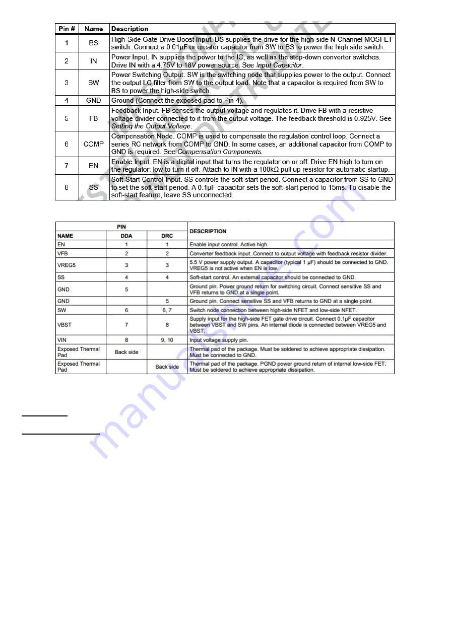
Table:

 Pin functions 


Table:

 Pin description 


TPS51363 

General Description  


The TPS51363 is a high-voltage input, synchronous converter with integrated FET, based on D-CAP2™ 

control topology, which enables fast transient response and supports both POSCAP and all MLCC output 

capacitors. TI proprietary FET technology combined with TI leading-edge package technology provides the 

highest density solution for single-output power rail such as VCCIO and VDDQ for DDR notebook memory, or 

any point-of-load (POL) in wide application. The feature set includes switching frequency of 400 kHz and 800 

kHz. Programmable soft-start time with an external capacitor. auto skip, pre-bias startup, integrated bootstrap 

switch, power good, enable and a full suite of fault protection schemes, including OCL, UVP, OVP, 5-V UVLO 

and thermal shutdown. It is packaged in 3.5 mm × 4.5 mm, 0.4-mm pitch, 28-pin QFN (RVE), and specified 

from -10°C to 85°C. 

Summary of Contents for 55293DLB

Page 1: ...HITACHI 55HK6T64U 55293DLB MB100 SERVICE MANUAL ...

Page 2: ...CK END PROCESSOR MSTAR 37 7 1Gb DDR3 SDRAM 41 8 2Gb DDR3 SDRAM 42 9 32Gbit 4G x 8 bit NAND Flash Memory 43 10 16M BIT 16M x 1 CMOS SERIAL FLASH EEPROM 45 11 Demodulator Stage 49 12 LNB supply and control IC 53 13 Troubleshootıng 54 A No Backlıght Problem 54 D CI Module Problem 56 E Stayıng ın Stand by Mode 58 F IR Problem 58 G Keypad Touchpad Problems 59 H USB Problems 59 İ No Sound Problem 60 J S...

Page 3: ...ofer output Common 1 Headphone Common 2x USB3 0 and 1xUSB2 0 Common 1 Ethernet RJ45 Common 1 External Touchpad Common Internal Wi Fi and BT 2 TUNER A SI2157 TERRESTRIAL AND CABLE TV TUNER Description The Si2157 is Silicon Labs fifth generation hybrid TV tuner supporting all worldwide terrestrial and cable TV standards Requiring no external balun SAW filters wirewound inductors or LNAs the Si2157 o...

Page 4: ...ng filters requiring no external inductors or SAW filters o Increased ESD protection on 6 pins Best in class real world reception o Exceeds MOPLL based tuners o Lowest phase noise o High Wi Fi and LTE immunity Low power consumption o 3 3 V and 1 8 V power supplies o 3 3 V single supply option Integrated power on reset circuit Single or separate output pins for ALIF DLIF connection to SoC Standard ...

Page 5: ...4 Table Pin Functions ...

Page 6: ...5 B M88TS2022 SATELLITE TUNER Pin Assigment ...

Page 7: ... to most digital audio processors and MPEG decoders The device accepts a wide of input data and data rates A fully programmable data path routes these channels to the internal speaker drivers The TAS5717 9 is a slave only device receiving all clocks from external sources The TAS5717 TAS5719 operates with a PWM carrier between a 384 kHz switching rate and a 352 KHz switching rate depending on the i...

Page 8: ...Biquads for Speaker EQ o Programmable Coefficients for DRC Filters o DC Blocking Filters o 0 125 dB Fine Volume Support General Features o Serial Control Interface Operational Without MCLK o Factory Trimmed Internal Oscillator for Automatic Rate Detection o Surface Mount 48 Pin 7 mm 7 mm HTQFP Package o AD BD and Ternary PWM Mode Support o Thermal and Short Circuit Protection Benefits o EQ Speaker...

Page 9: ...8 Pin descriptions and functions Figure TAS5719 Pin descriptions ...

Page 10: ...9 Table TAS5719 Pin Functions ...

Page 11: ...10 Table Recommended Operating Conditions B HEAD PHONE AMPLIFIER STAGE Head phone is a SoC single on chip configuration in mainboard Design scheme is shown in figure 3 Figure Head phone ...

Page 12: ...nsuring a pop free shutdown Using the DRV632 in audio products can reduce component count considerably compared to traditional methods of generating a 2 VRMS output The DRV632 does not require a power supply greater than 3 3 V to generate its 5 6 Vpp output nor does it require a split rail power supply The DRV632 integrates its own charge pump to generate a negative supply rail that provides a cle...

Page 13: ...and MPEG decoders The device accepts a wide range of input data and data rates A fully programmable data path routes these channels to the internal speaker drivers The TAS5727 is a slave only device receiving all clocks from external sources The TAS5727 operates with a PWM carrier between a 384 kHz switching rate amd a 288 kHz switching rate depending on the input sample rate Oversampling combined...

Page 14: ...essing Features o Programmable Coefficients for DRC Filters o DC Blocking Filters General Features o I2 C Serial Control Interface Operational Without MCLK o Requires Only 3 3 V and PVDD o No External Oscillator Internal Oscillator for Automatic Rate Detection o Surface Mount 48 Pin HTQFP Package o Thermal and Short Circuit Protection o 106 dB SNR A Weighted o AD BD and Ternary Modulation o Up to ...

Page 15: ...14 Table Electrical Characteristics Figure PHP Package Top View ...

Page 16: ...15 Table Pin Functions ...

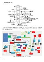
Page 17: ...d for taking voltages which are 12V 5V and 24V VDD_Audio These voltages are produced in power board Also socket is used for giving dimming backlight and standby signals with power board It is shown in figure 7 Figure General illustration of voltage stages on main board ...

Page 18: ... a proprietary circuit that enables the device to adopt to both low equivalent series resistance ESR output capacitors such as POSCAP or SP CAP and ultra low ESR ceramic capacitors The device operates from 4 5 V to 18 V VIN input The output voltage can be programmed between 0 76 V and 6 V The device also features an adjustable soft start time The TPS54528 is available in the 8 pin DDA package and ...

Page 19: ...with a cost effective low component count low standby current solution The main control loop for the TPS54328 uses the D CAP2 mode control that provides a fast transient response with no external compensation components The adaptive on time control supports seamless transition between PWM mode at higher load conditions and Eco mode operation at light loads Eco mode allows the TSP54328 to maintain ...

Page 20: ... Output Capacitor Wide VIN Input Voltage Range 4 5 V to 18 V Output Voltage Range 0 76 V to 7 V Highly Efficient Integrated FETs Optimized for Lower Duty Cycle Applications 100 mOhm High Side and 70 mOhm Low Side High Efficiency less than 10 mikroAmper at shutdown High Initial Bandgap Reference Accuracy Adjustable Soft Start Pre Biased Soft Start 700 kHz Switching Frequency fSW Cycle By Cycle Over...

Page 21: ...hnology provides the highest density solution for single output power rail such as VCCIO and VDDQ for DDR notebook memory or any point of load POL in wide application The feature set includes switching frequency of 400 kHz and 800 kHz Programmable soft start time with an external capacitor auto skip pre bias startup integrated bootstrap switch power good enable and a full suite of fault protection...

Page 22: ...SCAP and All MLCC Output Capacitor Usage Integrated and Temperature Compensated Low Side On Resistance Sensing for Accurate OCL Protection Powergood Output OCL OVP UVP and UVLO Protections Thermal Shutdown non latch Output Discharge Function Table 1 Current Ratings Integrated Boost MOSFET Switch 28 Pin 3 5 mm 4 5 mm RVE QFN Package with 0 4 mm Pitch and 1 mm Height Applications Notebook Computers ...

Page 23: ...22 Figure Pin Description Table Pin functions ...

Page 24: ...ent limit which prevents current runaway There is also a low side sinking current limit which turns off the low side MOSFET to prevent excessive reverse current Hiccup protection will be triggered if the overcurrent condition has persisted for longer than the preset time Thermal hiccup protection disables the device when the die temperature exceeds the thermal shutdown temperature and enables the ...

Page 25: ...24 Table Recommended operating conditions Figure Pin Description ...

Page 26: ...d range Current mode operation provides fast transient response and eases loop stabilization Full protection features include OCP and thermal shut down The MP2234 requires a minimum number of readily available standard external components and is available in a space saving 8 pin TSOT23 package Features Wide 4 5V to 16V Operating Input Range 2A Load Current 100mΩ 40mΩ Low Rds on Internal Power MOSF...

Page 27: ...26 Thermal Shutdown Output Adjustable from 0 8V Available in an 8 pin TSOT 23 package Figure Pin description Table Pin functions ...

Page 28: ...enabled by other power systems Pulling and holding the EN voltage below 0 4V shuts off the output The APL5910 is available in a SOP 8P package which features small size as SOP 8 and an Exposed Pad to reduce the junction to case resistance to extend power range of applications Features Ultra Low Dropout o 0 12V Typical at 1AOutput Current 0 8V Reference Voltage High Output Accuracy o 1 5 over Line ...

Page 29: ...ith only two external resistors In addition it is also available in five fixed voltages 1 8V 2 5V 2 85V 3 3V and 5V The LM1117 offers current limiting and thermal shutdown Its circuit includes a zener trimmed bandgap reference to assure output voltage accuracy to within 1 The LM1117 series is available in LLP TO 263 SOT 223 TO 220 and TO 252 D PAK packages A minimum of 10µF tantalum capacitor is r...

Page 30: ...n 0 2 Max Load Regulation 0 4 Max Temperature Range o LM1117 0 C to 125 C o LM1117I 40 C to 125 C Applications 2 85V Model for SCSI 2 Active Termination Post Regulator for Switching DC DC Converter High Efficiency Linear Regulators Battery Charger Battery Powered Instrumentation ...

Page 31: ...30 5 MICROCONTROLLER MSTAR MSD95C0H General Description ...

Page 32: ...31 Features ...

Page 33: ...32 ...

Page 34: ...33 ...

Page 35: ...34 ...

Page 36: ...35 ...

Page 37: ...36 Table Recommended operating conditions ...

Page 38: ...37 6 VIDEO BACK END PROCESSOR MSTAR MST7410DY General Description ...

Page 39: ...38 Table Recommended operating conditions Features ...

Page 40: ...39 ...

Page 41: ...40 Block Diagram Figure Block diagram ...

Page 42: ...l Data Strobe DQS DQS On chip DLL align DQ DQS and DQS transition with CK transition DM masks write data in at the both rising and falling edges of the data strobe All addresses and control inputs except data data strobes and data masks latched on the rising edges of the clock Programmable CAS latency 6 7 8 9 10 11 12 13 and 14 supported Programmable additive latency 0 CL 1 and CL 2 supported Prog...

Page 43: ...ential clock inputs CK CK operation Differential Data Strobe DQS DQS On chip DLL align DQ DQS and DQS transition with CK transition DM masks write data in at the both rising and falling edges of the data strobe All addresses and control inputs except data data strobes and data masks latched on the rising edges of the clock Programmable CAS latency 5 6 7 8 9 10 11 12 13 and 14 supported Programmabl...

Page 44: ...r rate up to 200MB s HS200 o MMC I F Clock frequency 0 200MHz o MMC I F Boot frequency 0 52MHz Operating voltage range o Vcc NAND 2 7 3 6V o Vccq Controller 1 7 1 95V 2 7 3 6V Temperature o Operation 25 C 85 C o Storage without operation 40 C 85 C Others o This product is compliance with the RoHS directive Supported features o HS200 o HPI BKOPS o Packed CMD Cache Data tag Context ID o Partitioning...

Page 45: ...ntroller e NAND has the built in intelligent controller which manages interface protocols wear leveling bad block management garbage collection and ECC e NAND protects the data contents from the host sudden power off failure e NAND is compatible with JEDEC standard eMMC4 5 specification ...

Page 46: ...active read current 10mA typical at 17MHz o Low active programming current 10mA typical o Low active erase current 10mA typical o Low standby current 30uA typical CMOS Minimum 100 000 erase program cycle Software Features Input Data Format o 1 byte Command code 3 byte address 1 byte byte address 512 byte Sequential Read Operation Built in 9 bit A0 to A8 pre settable address counter to support the ...

Page 47: ...segment is reached the device will wrap around to the beginning of the segment and continuously outputs data until CS goes high After program erase command is issued auto program erase algorithms which program erase and verify the specified page locations will be executed Program command is executed on a page 128 bytes basis and erase command is executed on both chip and sector 8K bytes basis To p...

Page 48: ...ta transfer rate o More than 100 000 erase program cycles o More than 20 year retention Efficient Continuous Read and QPI Mode o Continuous Read with 8 16 32 64 Byte Wrap o As few as 8 clocks to address memory o Quad Peripheral Interface QPI reduces instruction overhead o Allows true XIP execute in place operation o Outperforms X16 Parallel Flash Low Power Wide Temperature Range o Single 2 7 to 3 ...

Page 49: ...of 256 bytes each Up to 256 bytes can be programmed at a time Pages can be erased in groups of 16 4KB sector erase groups of 128 32KB block erase groups of 256 64KB block erase or the entire chip chip erase The W25Q32FV has 1 024 erasable sectors and 64 erasable blocks respectively The small 4KB sectors allow for greater flexibility in applications that require data and parameter storage The W25Q3...

Page 50: ...49 Table Pin description 11 DEMODULATOR STAGE MSB1240 DVB T2 Key Features ...

Page 51: ...50 General Description ...

Page 52: ...51 Block Diagram ...

Page 53: ...52 Pinning Absolute Maximum Ratings ...

Page 54: ... and I2C standard interfacing Key Features COMPLETE INTERFACE BETWEEN LNB AND I2C BUS BUILT IN DC DC CONVERTER FOR SINGLE 12V SUPPLY OPERATION AND HIGH EFFICIENCY TYP 93 0 5A SELECTABLE OUTPUT CURRENT LIMIT BY EXTERNAL RESISTOR COMPLIANT WITH MAIN SATELLITE RECEIVERS OUTPUT VOLTAGE SPECIFICATION ACCURATE BUILT IN 22 kHz TONE GENERATOR SUITS WIDELY ACCEPTED STANDARDS 22 KHz TONE WAVEFORM INTEGRITY ...

Page 55: ...e and backlight on the panel Possible couses Backlight pin dimming pin backlight supply stby on off pin BACKLIGHT_ON OFF pin should be high when the backlight is ON R23 must be low when the backlight is OFF If it is a problem please check Q35 and the panel cables Also it can be tested in TP310 in main board ...

Page 56: ... high or square wave in open position If it is low please check S268 for Mstar side and panel or power cables connectors Backlight power supply should be in panel specs Please check Q34 shown below also it can be checked TP149 ...

Page 57: ... collector D CI MODULE PROBLEM Problem CI is not working when CI module inserted Possible couses Supply suply control pin detect pins mechanical positions of pins CI supply should be 5V when CI module inserted If it is not 5V please check CI_PWR_CTRL this pin should be low ...

Page 58: ...57 Please check mechanical position of CI module Is it inserted properly or not Detect ports should be low If it is not low please check CI connector pins CI module pins ...

Page 59: ...tect pin should be logic high while normal operation When there is a short circuit protect pin will be logic low If you detect logic low on protect pin unplug the TV set and control voltage points with a multimeter to find the shorted voltage to ground F IR PROBLEM Problem LED or IR not working Check LED card supply on MB100 chasis ...

Page 60: ...D PROBLEMS Problem Keypad or Touchpad is not working Check keypad supply on MB100 H USB PROBLEMS Problem USB is not working or no USB Detection Check USB Supply It should be nearly 5V Also USB Enable should be logic high ...

Page 61: ...aker outputs Check supply voltages of 24V VDD_AUDIO 3 3V AUDIO_AVDD and AUDIO_DVDD with a voltage meter There may be a problem in headphone connector or headphone detect circuit when headphone is connected speakers are automatically muted Measure voltage at HP_DETECT pin it should be 3 3v ...

Page 62: ...ut SW Try to update TV with latest SW Additionally it is good to check SW printouts via Teraterm These printouts may give a clue about the problem You can use mini scart for terraterm connection K NO SIGNAL PROBLEM Problem No signal in TV mode Check tuner supply voltage 5V_VCC 3V3_TUNER and 1V8_TUNER Check tuner options are correctly set in Service menu Check AGC voltage at IF_AGC pin of tuner ...

Page 63: ...62 ...

Page 64: ... 1 3V3_VCC_TUNER DIFP M IN HDMI 4 TMDS_4 I2C_4 I2C USB1 3 0 CI Hotel TV RJ12 Subwoofer TAS5727 Audio Amp SAT_ADC LNA BGU7045 Slim SAV YPbPr Audio R L In BLUETOOTH SG HP SPK AIR MOUSE SLIM SCART TPS2553 USB Power Supply Switch USB1 WOWL_DET RAM INTERFACE Dimming_Main ATV DSP_SUB_OUT SUBW Pre Amp Small SubW Out HP LINEOUT SC AUDIO_OUT M88TS2002 Digital Satellite Tuner I2C 3V3_VCC 1V25_VCC LNBP LNBH2...

Page 65: ...64 15 PLACEMENT OF BLOCKS ...

Page 66: ...V5_VCC C2280 8n2 50V C2156 1u 16V F63 60R VFB_1V_CPU R426 10k 2 1 F64 60R R437 10k 2 1 C2211 22u 6V3 1u5 L26 C2212 22u 6V3 TPS54528 U46 5 6 7 8 4 3 2 1 EN VFB VREG5 VSS VIN VBST SSW GND 6V3 22u C2213 C1434 22p 50V 100n 16V C1271 22u 16V C2256 C1272 16V 100n 24V_VCC S220 STBY_ON OFF 12V_STBY 12V_STBY 12V_STBY 5V_STBY BACKLIGHT_ON OFF DIMMING VDD_AUDIO S118 S221 CN65 1 2 3 4 5 6 7 8 9 10 11 12 13 14...

Page 67: ...220k 120R R577 R578 120R 150R R579 150R R580 50V 1n C2019 C2020 1n 50V 50V C1543 0p5 C1544 50V 0p5 50V 2n2 C2115 50V C2116 2n2 RF1 RF2 BGU7045 U9 1 2 3 6 5 4 CTRL GND IN NC VCC OUT S151 3V3_LNA 3V3_LNA C1934 10V 100n 4k7 R83 R82 4k7 10n 16V C1553 RF2 RF1 10n 16V C1554 18R R581 1k5 F152 16V 10n C1555 FEF_AGC_FREEZE_D2 LNA_CTRL TPS2553 1 U6 1 2 3 6 5 4 FAULT ILIM OUT EN GND IN 5V_VCC R80 4k7 R334 56...

Page 68: ...848B Q64 C1530 50V 1n C1541 3p3 50V C1531 1n 50V 1n 50V C1532 C1545 50V 0p5 LNB_OUT S2_TUN_3V3 3k3 R530 16V C1556 10n 4n7 L5 S2_AGC_D1 100p 50V C1575 C1557 16V 10n C1558 16V 10n C1559 10n 16V S2_SCL_D1 S2_SDA_D1 QP_D1 QM_D1 IM_D1 IP_D1 33R R308 33R R309 50V C2001 18p 18p C2002 50V S2_TUN_3V3 S2_TUN_3V3 X2 27MHz 3 1 4 2 C1560 16V 10n 16V 10n C1561 10n C1562 16V 10k R484 S2_TUN_3V3 27p C1472 50V 50V...

Page 69: ...S_SDA VDD_1 GND_4 VDD33_1 MSPI_CLK SSPI_CSZ RESETZ GND_5 MSPI_DI SSPI_DO MSPI_DO SSPI_DI MSPI_CSZ SSPI_CLK TS_CLK TS_D 7 TS_D 6 DISEQC_IN1 VDD33_0 GND_3 I2CM_SDA I2CM_SCL GPIO 0 GND_2 VDD_0 DISEQC_OUT1 QM_S QP_S AVDD33_1 IM_S IP_S GND_1 IM_T IP_T IFAGC_T IFAGC_S AVDD33_0 XTAL_IN XTAL_OUT GND_0 I2CS_SCL S2_SDA_D2 S2_SCL_D2 DTV_SDA DTV_SCL 1V15_VCC_SAT VDD33_D2 VDD33_D2 AVDD33_D2 3V3_VCC_RF 10V C196...

Page 70: ...C16GTH 1 2 3 4 5 6 7 8 10k R472 R473 10k 75R R377 R378 75R D30 BAV70 C1469 27p 50V 5V_VCC R612 510R VGA_G VGA_R VGA_B 10V 100n C1950 1 2 VGA_DDC_5V TP193 TP194 TP195 VGA_DDC_5V TP196 S155 TP197 VGA_HSNC VGA_VSNC 75R R379 R650 100R 8 7 6 5 4 3 2 1 R4 R1 R3 R2 TP198 TP199 TP200 TP201 TP202 50V 27p C1470 C1471 27p 50V 510R R613 2k4 R651 10k R474 U14 ST24LC21 8 7 6 5 4 3 2 1 A0 A1 A2 GND SDA SCL WP VC...

Page 71: ...0 HSYNC0 VSYNC0 RIN1M RIN1P GIN1M GIN1P BIN1M BIN1P SOGIN1 HSYNC1 VSYNC1 RIN2M RIN2P GIN2M GIN2P BIN2M BIN2P SOGIN2 HSYNC2 VCOM CVBS0 CVBS1 CVBS2 CVBSOUT1 TN TP RN RP GPIO80 GPIO79 HWRESET XIN XOUT IRIN DM_P0 DP_P0 DM_P1 DP_P1 DM_P2 DP_P2 SSUSB_TXP1 SSUSB_TXN1 DM_PSS1 DP_PSS1 SSUSB_RXP1 SSUSB_RXN1 SSUSB_TXP0 SSUSB_TXN0 DM_PSS DP_PSS SSUSB_RXP0 SSUSB_RXN0 1 LED3 S213 1 2 LED1 BC848B Q69 R515 10k2 1...

Page 72: ... LM4675SD 5 6 7 8 4 3 2 1 IN IN VDD SHDN VO2 PVDD GND VO1 VDD_Bath 270k R656 270k R657 R695 33k 33k R696 10k R500 R501 10k 10V 4u7 C2178 10V C2179 4u7 560R R337 C1570 16V 10n 10n 16V C1571 560R R338 Bathroom_L Bathroom_R 100R R274 10u C1259 16V C1260 16V 10u 33R R313 Bathroom_IN R314 33R Bathroom_R Bathroom_L 16V 10u C1261 15u L23 F158 220R VDD_Bath 5V_VCC 3V3_STBY 1u 50V C2192 C1507 10u 6V3 C1417...

Page 73: ..._CLE NAND_ALE NAND_WEZ NAND_WPZ 3V3_NAND 3k9 R736 3V3_NAND R357 75R NAND_AD4 NAND_AD5 NAND_AD6 NAND_AD7 75R R358 R359 75R 75R R360 3V3_NAND NAND_AD0 NAND_AD1 NAND_AD2 NAND_AD3 75R R361 R362 75R 75R R363 R364 75R 75R R365 NF_DQS NAND128 A U31 1 2 3 4 5 6 7 8 9 10 11 12 13 14 15 16 17 18 19 20 21 22 23 24 25 26 27 28 29 30 31 32 33 34 35 36 37 38 39 40 41 42 43 44 45 46 47 48 NC29 NC28 NC27 NC26 I O...

Page 74: ...16 1 C2235 6V3 220u USB_1_VCC 16V C1239 100n USB1_TXN USB1_TXP R134 10R 2 1 10R R135 2 1 D37 AZ1065 06Q 8 7 6 5 4 3 2 1 P1 P2 P3 P4 P5 P6 GND VDD ESD USB1_RXP USB1_RXN USB1_DN USB1_DP TP17 1 TP18 1 USB_2_VCC TP19 1 TP20 1 TP21 1 TP22 1 F136 330R C2033 10u 10V USB_3_VCC USB3_DN USB_3_VCC 10R R138 2 1 C2034 10V 10u USB3_DP R139 10R 2 1 AZ099 04S U29 6 5 4 3 2 1 IO1 GND IO2 IO3 VDD IO4 5V_VCC USB_ENA...

Page 75: ...0u C1256 16V C1408 100n 16V AUVAG AUVRM AUVRM AUVAG R353 22R I2S_OUT_SD I2S_OUT_BCK I2S_OUT_MCK I2S_OUT_WS C1436 22p 50V R354 22R R355 22R 22RR356 50V 22p C1437 50V 22p C1438 50V C1439 22p HP_OUT_L_MSTAR DSP_SC_R_OUT DSP_SC_L_OUT HP_OUT_R_MSTAR SPDIF_OUT DSP_SUB_R_OUT DSP_SUB_L_OUT SC_AUD_L_IN SC_AUD_R_IN SAV_R_IN SAV_L_IN YPBPR_L YPBPR_R 2N7002 Q76 5V_STBY HDMI_CEC CEC 3V3_STBY 3V3_STBY JK6 1 2 3...

Page 76: ...3N R411 10k PANEL_VCC OP_PIN_V2 R677 33k R226 100R PAN_SCL OP_PIN13 R678 33k PANEL_VCC R412 10k 3D_EN S56 S57 3D_EN TX_V4P LA3P TX_V5N LA4N TX_V5P LA4P 1k F184 1k F170 1k F172 F185 1k 1k F186 F187 1k 1k F188 F189 1k 1k F190 F191 1k OP_PIN_V3 S345 OP_PIN36 OP_PIN35 F194 60R F195 60R TX_LB3N LOCK TX_LB3P HTPD S61 R900 10k R901 33k PANEL_VCC PAN_SDA S303 OP_PIN28 OP_PIN29 OP_PIN30 OP_PIN31 TX_V0P LA0...

Page 77: ... 100n C1858 AVDDL_USB3 100n C1859 220R F75 1V_VCC_CORE AVDDL_MOD_G6 C1860 100n F76 220R 1V_VCC_CORE_1 100u C2247 6V3 1V_VCC_CPU 100n C1867 100n C1868 100n C1869 100n C1870 C1871 100n C1872 100n C1873 100n 100n C1874 10u C2074 100n C1875 3V3_STBY 220R F77 100n C1896 100n C1897 AVDD_PLL_C 3V3_VCC_G6 F89 220R 100n C1898 C2078 4u7 6V3 C1899 100n AVDD3P3_MHL3 3V3_VCC 220R F90 C1900 100n 6V3 4u7 C2079 1...

Page 78: ... DDR12_RASB DDR1_DQL0 DDR1_DQL1 DDR1_DQL2 DDR1_DQL3 DDR1_DQU0 DDR1_DQL4 DDR1_DQL5 DDR1_DQL6 DDR1_DQL7 DDR1_DQU1 DDR1_DQU2 DDR1_DQU3 DDR1_DQU4 DDR1_DQU5 DDR1_DQU6 DDR12_A00 DDR12_A01 DDR12_A02 DDR12_A03 DDR12_A04 DDR12_A05 DDR12_A06 DDR12_A07 DDR12_A08 DDR12_A09 DDR12_A10 DDR12_A11 DDR12_A12 DDR12_A13 DDR1_DQU7 DDR12_A15 R803 56R 10n 16V C1550 R804 56R DDR12_CKB DDR12_CK DDR12_CKE DDR12_A14 R116 1k...

Page 79: ...DDR4_DQL7 DDR4_DQL6 DDR4_DQL5 DDR4_CKB 22R R348 22R R349 DDR4_CK DDR4_DQL4 DDR4_DQL3 DDR4_DQL2 DDR34_CK DDR34_CKB DDR4_CK DDR56_A04 DDR56_A03 DDR3_CSB DDR4_DQL1 DDR4_DQL0 DDR56_ODT U42 H5TQ2G63BFR PB N3 P7 P3 N2 P8 P2 R8 R2 T8 R3 L7 R7 N7 T3 J1 L1 M7 L9 T7 J9 M2 N8 M3 J7 K7 K9 L2 J3 K3 L3 T2 L8 H9 H2 F1 E9 D2 C9 C1 A8 A1 R9 R1 N9 N1 K8 K2 G7 D9 B2 H1 M8 E3 F7 F2 F8 H3 H8 G2 H7 D7 C3 C8 C2 A7 A2 B8...

Page 80: ...01 R629 100R 1 2 3 4 5 6 7 8 R1 R2 R3 R4 R932 100R DDR12_A07 DDR12_A09 DDR12_A13 C1795 100n 10V 10V 100n C1787 C1788 100n 10V C1789 100n 10V C1790 10V 100n C1791 10V 100n 10V 100n C1792 10V 100n C1796 C1797 100n 10V 10V 100n C1798 C1799 100n 10V 100RR933 R937 100R DDR12_BA2 DDR12_BA0 DDR12_A15 DDR12_WEB R934 100R 100RR946 C1800 100n 10V DDR12_ODT DDR12_RESETB DDR2_CK DDR2_CKB S126 S127 DDR34_RESET...

Page 81: ... AB16 AB15 AB14 AB12 AB8 AB7 AA30 AA25 AA20 AA19 AA18 AA15 AA14 AA13 AA12 AA8 AA7 AA3 Y30 Y27 Y26 Y25 Y20 Y19 Y18 Y15 Y14 Y13 Y12 Y8 Y7 VSS_303 VSS_304 VSS_305 VSS_306 VSS_307 VSS_308 VSS_309 VSS_310 VSS_311 VSS_312 VSS_313 VSS_314 VSS_315 VSS_316 VSS_317 VSS_318 VSS_319 VSS_320 VSS_321 VSS_322 VSS_323 VSS_324 VSS_325 VSS_326 VSS_327 VSS_328 VSS_329 VSS_330 VSS_331 VSS_332 VSS_333 VSS_334 VSS_335 ...

Page 82: ..._DQU2 A_DQSUB A_DQU4 A_DQU0 A_DQU6 A_DQSU A_DQSLB A_DQSL A_DQU1 A_DMU A_DQU5 A_DQU3 A_DQU7 A_DQL0 A_DQL2 A_DQL6 A_DQL4 R810 240R U36 H5TQ2G63BFR PB N3 P7 P3 N2 P8 P2 R8 R2 T8 R3 L7 R7 N7 T3 J1 L1 M7 L9 T7 J9 M2 N8 M3 J7 K7 K9 L2 J3 K3 L3 T2 L8 H9 H2 F1 E9 D2 C9 C1 A8 A1 R9 R1 N9 N1 K8 K2 G7 D9 B2 H1 M8 E3 F7 F2 F8 H3 H8 G2 H7 D7 C3 C8 C2 A7 A2 B8 A3 F3 G3 B7 C7 E7 D3 K1 G9 G1 F9 E8 E2 D8 D1 B9 B1 ...

Page 83: ... GPIO8 HDMI0_RXHPD GPIO9 HDMI2_RXCEC GPIO10 HDMI2_RXHPD GPIO11 RXHTPDN_OSD GPIO12 RXHTPDN_VID GPIO13 HDMI1_TXCEC GPIO14 RXLOCKN_OSD GPIO15 RXLOCKN_VID GPIO16 HDMI1_TXHPD GPIO17 3 U30 MST7410DY AM31 AL32 AK30 AL31 AK29 AL30 AM29 AL29 AF27 AF28 AL9 AM9 AL8 AK9 AL7 AK8 AK7 AM7 AJ11 AJ10 AF31 AF32 AG30 AG31 AJ32 AH31 AK31 AJ31 AM5 AL6 AK5 AL5 AK4 AL4 AM2 AM3 AL2 AL1 AK2 AL3 AJ2 AK3 AJ3 AJ1 HDMI0_RXCP ...

Page 84: ... 15 2 16 6 N1 N2 N3 DRAIN_M U200 TCET1102G 4 3 2 1 D201 C12V PIN_14 R280 10k FB_M 12V_STBY 1k R236 TL431SAMF2 U203 D204 C6V8 Q204 BC848B ST_BY 1n 50V C230 1k R255 1k R211 1k R223 12V_STBY 1k R237 1n C202 50V 1k R244 1n 50V C201 C2613 1n2 50V 12V_AC PIN_9 24V_AC D209 D210 D207 D208 1N4148 D105 12V_STBY_MB 12V_AC 24V_AC 25V 1m C209 C210 1m 25V 25V 1m C211 C212 1m 25V L200 1u 12V_STBY 24V_AC 12V_AC P...

Page 85: ...0R R310 R312 10R 10R R322 24 80V_FB 10R R569 10R R330 R339 10R 10R R301 R313 10R 10R R323 R331 10R R340 10R R302 10R 10R R314 R324 10R R332 10R R341 10R 10R R303 10R R315 10R R325 10R R333 10R R570 24 80V R571 10R R572 10R F1 800R 24V_AUDIO Q506 BSH103 S577 S578 10R R573 D307 1N4148 R307 100R V_20 10R R348 R527 10R R355 10R D310 C5V1 SW_OFF_S S3 S4 swjump HS1 S514 R546 10R C550 1n 4kV PL6 PL5 GND3...

Page 86: ...S532 S504 S501 S511 LED3 LED2 LED4 LED3 LED2 LED1 LED4 LED1 LED3 LED2 LED1_S LED2_S LED4_S LED3_S V_LED V_LED CN501 1 2 3 4 5 6 7 Q510 LED1_S LED1 VCC_LED LED4 S500 LED2 LED1 2u2 10V C514 OVP_LED CS_LED Q500 BC858B 10R R202 SR4 S200 C234 1n 4kV R203 10R GND3 R200 10R 10R R201 C500 50V 1n C510 10V 2u2 VCC_LED GATE_LED GATE_LED D501 SB5100 D503 2D 3D OPS D114 RL207 R104 1M 1M R103 R102 1M R101 1M 07...

Reviews: