background image

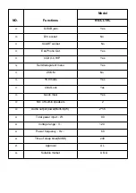
Model


NO. 

Functions NS-CL19C 


29 

D-SUB jack 

Yes 


30 

DVI socket 

No 


31 

SCART socket 

  No 


32 

Ear-Phone Out 

Yes 


33 

CCD,V-CHIP Yes 


34 

Semitransparent menu 

Yes 


35 

ZOOM No 


36 

16:9 mode 

Yes 


37 

Child Lock 

Yes 


38 

Quick View 

Yes 


39 

NO. of built-in speakers 


40 

Audio output power(Built-in)(W) 

2*1.5 


41 

Total power input

W


80 


42 

Voltage range

V


120 


43 

Power frequency

Hz


60 


44 

Time of sleep timer(MINS) 

240 


45 

Approval UL 


46 

Suitable market 

U.S.A 


Summary of Contents for NS-CL19C

Page 1: ...NS CL19C ...

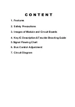
Page 2: ...1 Features 2 Safety Precautions 3 Images of Module and Circuit Boards 4 Key IC Description Trouble Shooting Guide 5 Signal Flowing Chart 6 Bus Control Adjustment 7 Circuit Diagram ...

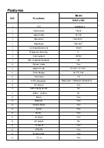
Page 3: ...ystem NTSC 9 NO of preset channels 181 10 Picture mode Yes 11 Angel of view H 160 V 160 12 Color display 16 777 216 13 Color level 16 14 OSD languages ENGLISH FRENCH SPANISH 15 AV stereo Yes 16 Surrounding sound No 17 Audio system M 18 Bass Yes 19 Balance Yes 20 Sound mode Yes 21 Mute Yes 22 BTSC Yes 23 AV input Yes 24 AV output No 25 Y CB CR Yes 26 Y PB PR Yes 27 S video jack Yes 28 TV in Yes ...

Page 4: ...CHIP Yes 34 Semitransparent menu Yes 35 ZOOM No 36 16 9 mode Yes 37 Child Lock Yes 38 Quick View Yes 39 NO of built in speakers 2 40 Audio output power Built in W 2 1 5 41 Total power input W 80 42 Voltage range V 120 43 Power frequency Hz 60 44 Time of sleep timer MINS 240 45 Approval UL 46 Suitable market U S A ...

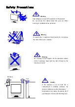
Page 5: ...rd Do not expose the main unit to rain or moisture Warning Do not drop or push objects into the television cabinet slots or openings Never spill any kind of liquid on the television receiver Caution If the television is to be built into a compartment or similarly enclosed the minimum distances must be maintained Heat build up can reduce the service life of your television and can also be dangerous...

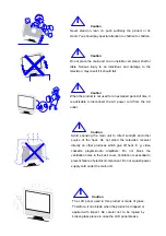
Page 6: ... the AC outlet Caution Avoid exposing the main unit to direct sunlight and other source of the heat Do not stand the television receiver directly on other produces which give off heat E g video cassette players Audio amplifiers Do not block the ventilation holes in the back cover Ventilation is essential to prevent failure of electrical component Do not squash power supply cord under the main unit...

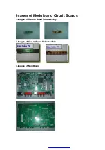
Page 7: ...Images of Module and Circuit Boards 1 images of Remote Board Subassembly 2 images of Control Panel Subassembly 3 images of Main Board ...

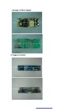
Page 8: ...4 images of Power Supply 5 images of Inverter ...

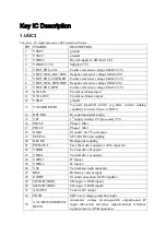
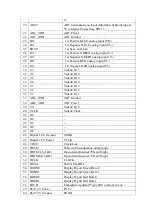
Page 9: ...ty for direct drive of LEDs 14 DECDIG Decoupling digital supply 15 VP1 1st supply voltage TV processor 5V 16 PH2LF Phase 2 filter 17 PH1LF Phase 1 filter 18 GND1 Ground 1 for TV processor 19 SECPLL SECAM OLL decoupling 20 DECBG Bandgap decoupling 21 EWD AVL East West drive output or AVL capacitor 22 VDRB Vertical drive B output 23 VDRA Vertical drive A output 24 VIFIN1 IF input 1 25 VIFIN2 IF inpu...

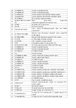
Page 10: ...left signal 50 AUDIOIN4R Audio 4 input right signal 51 CVBS4 Y4 CVBS4 Y4 input 52 C4 Chroma 4 input 53 AUDIOIN2L SSIF Audio 2 input left signal sound IF input 54 AUDIOIN2R Audio 2 input right signal 55 CVBS2 Y2 CVBS2 Y2 input 56 AUDIOIN3L Audio 3 input left signal 57 AUDIOIN3R Audio 3 input right signal 58 CVBS3 Y3 CVBS 3 Y2 input 59 C2 C3 Chroma 2 3 input 60 AUDOUTLSL Audio output for audio power...

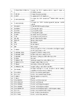
Page 11: ...ence voltage 0V 90 VREFAD_POS Positive reference voltage 3 3V 91 VREFAD Reference voltage for audio ADCs 3 3 2V 92 GNDA Ground 93 VDDA 1 8V Analogue supply for audio ADCs 1 8v 94 VDDA2 3 3V Supply voltage SDAC 3 3V 95 VSSadc Ground for video ADC and PLL 96 VDDadc 1 8V Supply voltage video ADC and PLL 97 INTO P0 5 External interrupt 0 or port 0 5 4mA current sinking capability for direct drive of L...

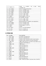
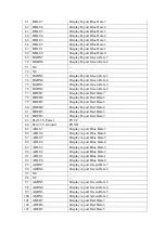
Page 12: ...P1 2 INT2 Port 1 2 or external interrupt 2 127 P1 4 RX Port 1 4 or UART bus 128 P1 5TX Port 1 5 or UART bus 2 RTD2023B PIN SYMBOL DESCRIPTION 1 APLL_GND Ground for multi phase PLL 2 APLL_VDD Power for multi phase PLL 3 PLL_TEST1 Test Pin 1 Power on latch for MCU crystal location 4 PLL_TEST2 Test Pin 2 Power on latch for crystal in frequency 5 TMDS_TST TMDS_TEST Pin Power on latch for host interfac...

Page 13: ... bit 4 34 V3 Video8 bit 3 35 V2 Video8 bit 2 36 V1 Video8 bit 1 37 ADC_GND ADC Ground 38 ADC_VDD ADC Power 39 V0 Video8 bit 0 40 VCLK Video8 Clock 41 NC 42 NC 43 NC 44 NC 45 NC 46 Digital 1 8V Ground GNDK 47 Digital 1 8V Power VCCK 48 COUT Crystal out 49 PWM2 Pulse width modulation output port2 50 DDCSCL1 ADC Open drain Internal 75K pull high 51 DDCSDA1 ADC Open drain Internal 75K pull high 52 DCL...

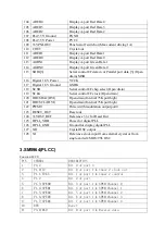
Page 14: ...play B port Red Data 5 80 BRED4 Display B port Red Data 4 81 BRED3 Display B port Red Data 3 82 BRED2 Display B port Red Data 2 83 Pad 3 3V Power PVCC 84 Pad 3 3V Ground PGND 85 ABLU7 Display A port Blue Data 7 86 ABLU6 Display A port Blue Data 6 87 ABLU5 Display A port Blue Data 5 88 ABLU4 Display A port Blue Data 4 89 ABLU3 Display A port Blue Data 3 90 ABLU2 Display A port Blue Data 2 91 ABLU1 ...

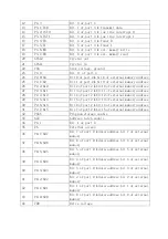
Page 15: ... drain Internal 75K pull high 121 DDCSCL2 DVI Open drain Internal 75K pull high 122 PWM0 Pulse width modulation output port0 123 RESET_OUT Reset out 124 33VRST_REF Reference 3 3v for Reset Out 125 DPLL_VDD Power for digital PLL 126 DPLL_GND Ground for display digital PLL 127 XO Crystal OSC output 128 XI Reference clock input from external crystal or from single ended CMOS TTL OSC 3 SM5964 PLCC Fun...

Page 16: ... port 2 bit 12 of external memory address 29 P2 5 A13 Bit 5 of port 2 bit 13 of external memory address 30 P2 6 A14 Bit 6 of port 2 bit 14 of external memory address 31 P2 7 A15 Bit 7 of port 2 bit 15 of external memory address 32 PSEN Program storage enable 33 ALE Address latch enable 34 P4 1 Bit 1 of port 4 35 EA External access 36 P0 7 AD7 Bit 7 of port 0 data address bit 7 of external memory 3...

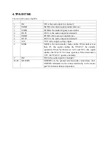
Page 17: ...channel 2 7 VCC VCC is the supply voltage input 8 M SB M SB is the mute standby mode enable When held at less than 2V this signal enables the TPA1517 for standby operation When held between 3 4V and 8 8V this signal enables the TPA1517 for mute operation When held above 9 2V the TPA1517 operates normally 9 IN2 IN2 in the audio input for channel 2 10 20 GND HS GND HS are the ground and heat sink co...

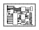
Page 18: ...PU 5V 74LVC14 TVR TVG TVB VGA_SCL VGA_SDA VGA_SCL VGA_SDA SCL SDA SDA SCL 24C16 TDQ 6H3 MUTE AMP STB DC_12V TV VS TV HS TV HS TV VS DVD_PW DVD5V MP1410 MP1410 DVD_PW MUTE AMP STB PW_DN YP VGA SEL CPU 5V IR LED RED LED GRN K0 K1 U_8V DVD12V DVD5V K2 K3 K4 K5 K6 SC RST CBT3257 Y Pb Pr U_1V8 U_3V3 S_3V3 U_1V8 S_3V3 U_3V3 TUNER TVR TVG TVB AUDIO LOUT AUDIO ROUT OPTION UOC_SDA UOC_SCL UOC_REQCOMM UOC_R...

Page 19: ... BS 1 IN 2 SW 3 GND 4 FB 5 COMP 6 EN 7 NC 8 U15 MP1410ES SO 8 C164 100pF 0603 NPO 5 50V C147 0 01uF 0603 X7R 10 50V R66 10Kohm 0603 5 1 10W C146 0 01uF 0603 X7R 10 50V R190 30 9Kohm 0603 1 1 10W R191 10Kohm 0603 5 1 10W C198 0 1uF 0603 Y5V 80 20 50V VI 3 GND 2 VO 1 U7 78L05 SOT 89 H1 TEST H2 TEST CPU5V DC_PW DC2_PW R36 NC 270ohm 0603 5 1 10W A K D11 NC 3 3V E102 47uF 25V 20 5 7 105 L18 GZ1608D121T...

Page 20: ...NPO 5 50V C11 100pF 0603 NPO 5 50V C12 100pF 0603 NPO 5 50V C13 100pF 0603 NPO 5 50V C17 100pF 0603 NPO 5 50V SDIO DVD_STB DVD_CLK DVD_IR DVD_DAT GND 1 2 3 4 5 CN19 NC 5PIN 2 0 D H R83 NC 330ohm 0603 5 1 10W IR_IN LED_O LED_G PPWR BACKLIGHT_PW R263 4K7ohm 0603 5 1 10W R264 4K7ohm 0603 5 1 10W R266 510ohm 0603 5 1 10W R265 510ohm 0603 5 1 10W CPU5V Q1 MMBT3906 2A SOT 23 Q2 MMBT3906 2A SOT 23 C144 0...

Page 21: ...1 MMBT3906 2A SOT 23 E46 100uF 16V 20 5 11 105 GND R220 10Kohm 0603 5 1 10W R229 240ohm 0603 5 1 10W R49 1Kohm 0603 5 1 10W GND D14 LL4148 LL 34 R231 4K7ohm 0603 5 1 10W R244 1K2ohm 0603 5 1 10W R245 5K6ohm 0603 5 1 10W R221 10Kohm 0603 5 1 10W GND C120 0 1uF 0603 Y5V 80 20 50V GND GND MUTE AMP_STB GND GND R246 68Kohm 0603 5 1 10W E60 47uF 25V 20 5 7 105 GND R222 10Kohm 0603 5 1 10W GND R225 NC 10...

Page 22: ...34 10Kohm 0603 5 1 10W R133 10Kohm 0603 5 1 10W 12V C148 0 22uF 0603 Y5V 80 20 16V E69 10uF 25V 20 5 11 105 C155 3300pF 0603 X7R 10 50V R204 390ohm 0603 5 1 10W C75 0 1uF 0603 Y5V 80 20 50V E70 1uF 50V 20 5 11 105 E68 2 2uF 50V 20 5 11 105 8V C77 0 1uF 0603 Y5V 80 20 50V C128 0 1uF 0603 Y5V 80 20 50V 3 5 6 7 26 54 92 R216 100ohm 0603 5 1 10W R217 100ohm 0603 5 1 10W C86 0 1uF 0603 Y5V 80 20 50V L3...

Page 23: ...m 0603 5 1 10W R150 6K8ohm 0603 5 1 10W D26 BA792L8 SOD110 A A K K D28 LL4148 LL 34 D25 BA792L8 SOD110 Q12 MMBT3904LT1 1A SOT 23 R140 NC 0ohm 0603 5 1 10W OP2 R99 100ohm 0603 5 1 10W C123 0 1uF 0603 Y5V 80 20 50V E30 47uF 25V 20 5 7 105 5V_IF L12 EC0410 101K R26 NC 2K2ohm 0603 5 1 10W E1 NC 47uF 50V 20 5 12 105 12V C48 NC 0 1uF 0603 Y5V 80 20 50V 1 3 2 D2 NC BAV99LT1 A7 SOT 23 C49 NC 0 01uF 0603 X...

Page 24: ...V C63 0 1uF 0603 Y5V 80 20 50V REF DVI_SCL DVI_SDA DAGRN0 DAGRN1 DAGRN2 DAGRN3 DAGRN4 DAGRN5 DAGRN6 DAGRN7 DARED6 DARED0 DARED2 DARED4 DARED1 DARED3 DARED5 DARED7 DABLU1 DABLU7 DABLU5 DABLU0 DABLU2 DABLU3 DABLU4 DABLU6 1 3 5 7 8 6 4 2 RP14 4 33ohm 0603 5 1 16W DHS DVS DE C60 10pF 0603 NPO 5 50V C57 10pF 0603 NPO 5 50V C61 10pF 0603 NPO 5 50V L2 GZ1608D121T 0603 CLK C62 27pF 0603 NPO 5 50V G0 G0 C3...

Page 25: ... DVD_AUD_L 1 2 3 CN22 3PIN 2 0 D H DVD_R_IN DVD_L_IN VGA_R VGA_G VGA_B VGA_SCL VGA_SDA VGAHS VGAVS 1 2 3 4 5 6 7 8 9 10 11 12 13 14 15 CN1 D341 015F 5A20A 长体 TXD RXD VGAVS VGAHS R4 100ohm 0603 5 1 10W C2 20pF 0603 NPO 5 50V R5 100ohm 0603 5 1 10W C1 20pF 0603 NPO 5 50V VGA_R VGA_G VGA_B VGA_VS VGA_HS R2 2Kohm 0603 5 1 10W R1 2Kohm 0603 5 1 10W 1 3 2 D4 BAV99LT1 A7 SOT 23 1 3 2 D5 BAV99LT1 A7 SOT 2...

Page 26: ... X7R 10 50V L48 SDFL1608Q2R2KT F 0603 C203 680pF 0603 X7R 10 50V L49 SDFL1608Q2R2KT F 0603 C202 330pF 0603 X7R 10 50V AV1 5V C121 100pF 0603 NPO 5 50V R86 47Kohm 0603 5 1 10W R69 1Kohm 0603 5 1 10W E10 2 2uF 50V 20 5 11 105 C118 100pF 0603 NPO 5 50V R85 47Kohm 0603 5 1 10W R71 1Kohm 0603 5 1 10W E12 2 2uF 50V 20 5 11 105 1 2 D21 MLVS0603M07 1 2 D9 MLVS0603M07 AV_AUD_L AV_AUD_R C228 0 1uF 0603 Y5V ...

Page 27: ... output for LDO OK Turn on or not Check the power supply net follow F1 Turn on the set Change LDO Or The load is OK Check Pin3 U13 For 350Khz switch signal U13 MP1410ES D17 IN5822 Check L9 47μH Higt Voltage Low voltage U13 MP1410ES 5thPIn U13 Check C111 0 01F Y N Y N N Y Y N Y N Y N N Y OK Check Mcu 1 power supply 2 Reset 3 Crystal N Y ...

Page 28: ...eck 5V for BLON on CN10 Tunn on or not Turn on 图 2 Check Mcu 1 power supply 2 Reset 3 Crystal Check the cirture for Q4 MMBT3904 N N N Y Y 12V inverter input Check the power supply Check the inverter or self proofed N Y Check U25 SM5964 43th PIN ...

Page 29: ...eck voltage of Q24 Turn to power suppy trouble shorting Check LCD or Panel Connector Check U5 1 Power supply 2 Time circuit Check Q24 0 3 3V 5V or 12V according to the volitage N Y Check power supply for panel Check voltage of Q24 Check Q24 be care for the shorting Check circuit between CN8 and CN9 N N N N Y Y Y Y ...

Page 30: ...k voltage for the panel Check the panel connector Check LCD Check the output net the connector Change the panel connector Change LCD Select the right panel voltage N Y N N Y Y Check U5 For Power supply timer circuit Y Change mend the part circuit N ...

Page 31: ...from C11 Y N Check the speaker N Y Check U25 SM5964 And U25 I 0 interface PIN6 12 Check U3 PIN1 and PIN9 for signal input Y N Y N Check U3 PIN4 and PIN6 for signal output Chekc U21PIN60 61for signal output Y N Check U3 or E45 100 Examine and repair the output net between U3 and CN11 Check net between U21 PIN60 61 And U3 PIN1 9 Check input audio input AV U21 PIN49 50 PC下 U21PIN53 54 Check U21 Check...

Page 32: ...ure Check audio and PC AV N Y Turn to NO AUDIO trouble shooting Check signal ouput of SAW2 M9370M30 PIN1 1 check SAW2 2 check U21 PIN29 30 3 check power supply of U21 4 change U21 Check the net between SAW2 Pin1and C133 0 01μF Check C133 Y N ...

Page 33: ...3 3 TV Audio abnormal Noise and NICAM can t be detected Check the audio system Select the right audio Search again Picture is normal Check C113 0 01UF D26 R140 0 or change SAW2 N N Y Y ...

Page 34: ...net Y N Check voltage T1 PIN3 for 0V Examine and repair R267 0Ω N Y Check I2 C signal T1 PIN4 5 Check I2 C net connect with U25 SM5964 PIN16 17 N Y Check signal T1 PIN11 N Check the net between T1 PIN11 and U21 PIN24 25 Power supply for U21 Y Check voltage T1 PIN1 V Examine and repair The circuit N Y Change T1 TDQ 6H3 Check voltage T1 PIN9 for 33V Examine and repair 33V circuit Y N ...

Page 35: ...PC Picture not in center Missing color Picture dithering No signal Auto adjust Check U5 RGB input Reset Y N Check R G B circuit Check VS HS signal Check OSD setting Reset Check VS HS i i Y N Check VS HS PC ...

Page 36: ...4 3 AV SV SCART YPbPr YCbCr S Video AV Missing color No signal No signal except PC Reset Check RGB circuit Check VS HS circuit Check the circuit for power supply of U21 Check RGB signal input for U5 Y N ...

Page 37: ...Sincere forever Tel 86 532 88938356 ...

Reviews: