background image

WARNING 

This service information is designed for experienced repair technicians only and is not designed for use 

by  the  general  public.  It  does  not  contain  warnings  or  cautions  to  advise  non-technical  individuals  of 

potential dangers in attempting to service a product. Products powered b electricity should be serviced 

or repaired only by experienced professional technicians. Any attempt to service or repair the product 

deal with in this service information by anyone else could result in serious injury or death

CONTENT 

1. SPECIFICATIONS………………………………………………………………………….. 3 

2. WAINING…………………………………………………………………………………….. 4 

3. LOCATION OF CONTROLS AND COMPONENTS…………………………………….. 6 

3.1.Board Location……………………………….. ………………………………….…….6 

3.2 Main Board & AV Board……………………………….. ……………………………..6 

3.3 Power Board……………………………….. …………………………………………11 

3.4 DC/DC Power Subassembly……………………………….. ……………………….12 

3.5 LCD Panel……………………………….. ……………………………………………13 

4. FEATURES AND TECHINICAL DESCRIPTION…………………………………………15 

5. INSTALLATION INSTRUCTIONS…………………………………………………………18 

5.1 External Equipment Connections………………………………….. ………………..18 

5.2 HDMI Connections……………………………….. ……………………………………22 

6. OPERATION INSTRUCTIONS…………………………………………………………….27 

6.1 Front Panel Controls……………………………….. ………………………………….27 

6.2 Back Panel Controls……………………………….. ………….………..…………….27 

6.3 Universal Remote Controller……………………………….. …..…………………….28 

7. DISASSEMBLY INSTRUCTIONS……………………………………..………………….36 

7.1 Whole Machine………………………………………………...……………………….36 

7.2 Base Subassembly……………………………………………..…….………………..37 

7.3 Back Subassembly…………………………………………..……….………………..38 

7.4 Screen bracket Subassembly……………………………..………………………….39 

7.5 Front frame Subassembly…………………………………………….………………40 

7.6 Wire Subassembly…………………………………………………………………….41 

8. MEASUREMENTS AND ADJUSTMENTS………………………………………………42 

9. BLOCK DIAGRAM AND CIRCUIT DIAGRAM…………………………………………..52 

9.1 Block Diagram……………………………………………………………………………52 

9.2 Circuit Diagram…………………………………………………………………………52 

10. WIRING CONNECTION DIAGRAM…………………………………………………….53 

10.1 Printed Circuit Board……………………………………………………….…………53 

10.2 Wiring Connection DIGRAM………………………………………………………….53 

11. TROUBLESHOOTING GUIDE…………………………………………………..……...53 

11.1. Simple check…………………………………………………………..…………...53 

11.2. PSU failure check…………………………………………………..………………54 

11.3. DC/DC board failure check………………………………………………...……...55 

11.4. Main board failure check…………………………………………………………. .55 


Summary of Contents for HLC15T

Page 1: ...HLC15T 1 ...

Page 2: ...oard 11 3 4 DC DC Power Subassembly 12 3 5 LCD Panel 13 4 FEATURES AND TECHINICAL DESCRIPTION 15 5 INSTALLATION INSTRUCTIONS 18 5 1 External Equipment Connections 18 5 2 HDMI Connections 22 6 OPERATION INSTRUCTIONS 27 6 1 Front Panel Controls 27 6 2 Back Panel Controls 27 6 3 Universal Remote Controller 28 7 DISASSEMBLY INSTRUCTIONS 36 7 1 Whole Machine 36 7 2 Base Subassembly 37 7 3 Back Subassem...

Page 3: ...11 5 Pannel failure 57 12 MAINTENANCE 60 3 ...

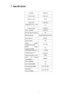
Page 4: ... preset channels 181 OSD language English Spanish French Color system NTSC Audio system M Audio output power Built in W 2 1 5W Audio output power outer W No Total power input W 50W Voltage range V AC120V Power frequency Hz 60Hz Time of sleep timer MINS 240Min Net weight KG 2 5 Gross weight KG 3 2 Net dimension MM 392 168 347 Packaged dimension MM 448 193 387 4 ...

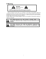
Page 5: ...tfrom being damaged the following rules should be observed for the installation use and maintenance of th product Read the following safety instruction before starting the operation The User Manual uses the following symbols to ensure a safe operation and preventany damage to operators or properties THIS SYMBOL INDICATES THAT HIGH VOLTAGE IS PRESENT INSIDE IT IS DANGEROUS TO MAKE ANY KING OF CONTA...

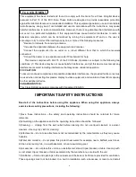
Page 6: ...ay cause undesired operation FCC CAUTION To assure continued compliance and possible undesirable interference the provided ferrite cores must be used when connecting this plasma display to video equipment and maintain at least 40cm spacing to other peripheral device CANADIAN NOTICE This Class B digital apparatus compiles with Canadian ICES 003 IMPORTANT SAFETY INSTRUCTIONS Read all of the instruct...

Page 7: ... surges 12 Never push objects of any kind into this product through openings as they may touch dangerous voltage point or short out parts that could result in a fire or electric shock Avoid spilling liquid of any kind on the product 13 Servicing do not attempt to service the product by yourself as opening or removing covers may expose you to dangerous voltage or other hazards Refer all servicing t...

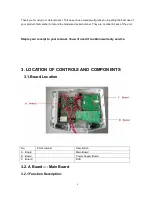
Page 8: ...he model and serial number They are on label in back of the unit Staple your receipt to your manual You will need it to obtain warranty service 3 LOCATION OF CONTROLS AND COMPONENTS 3 1 Board Location No Parts number Description A Board Main Board B Board Power Supply Board C Board DVD 3 2 A Board Main Board 3 2 1 Function Description 8 ...

Page 9: ...in 3 Backlight on off The system can turn on or turn off the backlight of TFT LCD Panel through the power supply unit path CN3 Pin 7 System power on standby System board will use this pin to control system power CN3 Pin 4 Control the luminance of backlight The system can generate the PWN signal to control the strength of TFT LCD Panel s backlight through this connector TFT LCD Panel LVDS Connector...

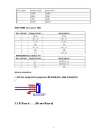
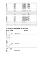
Page 10: ...XE3 LVDS EVEN 3 Signal 18 RXE3 LVDS EVEN 3 Signal 19 RXO0 LVDS ODD 0 Signal 20 RXO0 LVDS ODD 0 Signal 21 RXO1 LVDS ODD 1 Signal 22 RXO1 LVDS ODD 1 Signal 23 RXO2 LVDS ODD 2 Signal 24 RXO2 LVDS ODD 2 Signal 25 26 GND Ground 27 RXOC LVDS ODD Clock Signal 28 RXOC LVDS ODD Clock Signal 29 RXO3 LVDS ODD 3 Signal 30 RXO3 LVDS ODD 3 Signal Keypad and remote connector CN2 Speaker connector CN1 10 ...

Page 11: ...GND GND 5 PR_IN PR1 IN 6 GND GND 7 IR DVD IR DVD AUDIO Connector P1 Pin number Signal name Description 1 LI YPBPR1L_IN 2 RI YPBPR1R_IN 3 GND GND Other connectors 1 CN19 to Upgrade the program of MTK5380 U13 AND FLASH U17 J3 3V3SB 1 U0RX 2 U0TX 3 4 4x1 W HOUSING DIP4 W H P2 0 3 3 B Board Power Board 11 ...

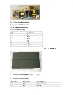
Page 12: ...3 2Connectordefinition INPUT CONNECTOR CN6 CN6 Signal name 1 N 2 GND 3 GND 4 DIM 5 EN 6 12V 7 12V 3 4 1 Function Description Display the signal 3 4 2 Connector definition 3 4 LCD PANNEL Pin number Signal name Description 1 3 Power Power for panel 4 6 GND Ground 12 ...

Page 13: ...O0 LVDS ODD 0 Signal 20 RXO0 LVDS ODD 0 Signal 21 RXO1 LVDS ODD 1 Signal 22 RXO1 LVDS ODD 1 Signal 23 RXO2 LVDS ODD 2 Signal 24 RXO2 LVDS ODD 2 Signal 25 26 GND Ground 27 RXOC LVDS ODD Clock Signal 28 RXOC LVDS ODD Clock Signal 29 RXO3 LVDS ODD 3 Signal 30 RXO3 LVDS ODD 3 Signal CN1 Header S14B PH SM4 TB D LF JST or equivalent Pin No Symnbol Description 1 2 3 VBL 3 3V Power input 4 5 6 13 14 25 26...

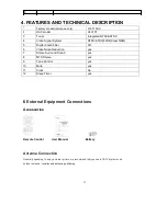
Page 14: ...mb Filter 3D 6 Video Noise Reduction yes 7 Stereo Surround Sound yes 8 MTS Stereo yes 9 Tone Control yes 10 Mute yes 11 Clock No 12 Sleep Timer yes 6 External Equipment Connections Accessories Remote Control User Manual Battery Antenna Connection Generally speaking to enjoy a clearer picture we recommend that you use a CATV system or an outdoor antenna location and antenna positioning 21 ...

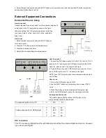
Page 15: ...on which is best for you VCR connection To avoid picture noise interference leave an adequate distance between the VCR and TV L R R L V S Video CVBS S Video CVBS Audio In AV OUT RF INP UT Connection Option 1 Set VCR output switch to channel 3 or 4 and then tune the TV to the same channel number Connection Option 2 1 Connect the audio and video cables from the VCR s output jacks to the TV input jac...

Page 16: ... connect 1 Connect the DVD video outputs Y Pb Cb Pr Cr to the Y Pb Pr jacks on the TV and connect the DVD audio outputs to the YPbPr Audio IN jacks on the TV as shown in the figure L R DVI Audio IN YPbPr Audio In Headphone out S Video CVBS S Video CVBS Audio In 2 If your DVD only has an S VIDEO output jack connect this to the S VIDEO input on the TV as shown in the figure NOTE If your DVD player d...

Page 17: ...the TV Digital Audio L R Optical Output port 2 Connect the other end of the optical cable to the digital audio optical input on the audio equipment See the external audio equipment instruction manual for operation Note When connecting with external audio equipments such as amplifiers or speakers please turn the TV speakers off Caution Do not look into the optical output port Looking at the laser b...

Page 18: ... the PC graphic card NOTES 1 Use a DVI cable 2 Avoid keeping a fixed image on the TV s screen for a long period of time The fixed image may become permanently imprinted on the screen 3 The synchronization input form for Horizontal and Vertical frequencies is separate R esolution Mode Resolution Frame frequency Hz VGA 640 480 60Hz SVGA 800 600 60Hz 75Hz 60Hz 75Hz XGA 1024 768 85Hz Connecting Headph...

Page 19: ...tlet do not attempt to file or cut the blade It is the user s responsibility to have an electrician replace the obsolete outlet If you cause a static discharge when touching the unit and the unit fails to function simply unplug the unit from the AC outlet and plug it back in The unit should return to normal operation Polarized AC Cord Plug Take the table stand off You can take off the table stand ...

Page 20: ...7 2 Back panel controls 27 ...

Page 21: ...7 3 Setting Up Your Remote Control 28 ...

Page 22: ...29 ...

Page 23: ...Subassembly Control Board Subassembly Assembly Material Subassembly Romoter Contral Per setting Subassembly 1 2 3 1 3 2 3 3 3 4 3 5 3 6 3 7 Components List NO Name Description Parts number 1 HLC15T whole machine 2 Packaging 3 1 Base subassembly 3 2 Rear cover subassembly 3 3 Front Frame Subassembly 3 4 Control Board Subassembly 3 5 Remote Control Board Subassembly 3 6 Mainboard Subassembly 3 7 DVD...

Page 24: ...pare Parts Name in English Specification Qty Base subassembly 1 Base pannel 1 Mat 4 Iron patch 1 Base subassembly Bolt SJ2824 87 ST3 10F 4 8 3 Rear cover subassembly Components List Subassembly Spare parts Location No Spare Parts Name in English Specification Qty 31 ...

Page 25: ...ear cover 1 Copper tessera 4 Rotate axis 1 Rotate axis board 1 Bolt SJ2825 87 ST3 6F 4 Terminal board 1 Rear terminal label 1 Bolt SJ2824 87 ST3X10F 3 Metal clip 3 Cloth 0 3 sponge bar 0 2 Bolt SJ2824 87 ST3X10F 6 Bolt SJ2824 87 ST3X10F 4 DVD Button Bracket 1 DVD Button Lable 1 Bolt SJ2822 87 ST3 10 2 Rear cover subassembly Bolt SJ2825 87 ST3 10F 4 32 ...

Page 26: ...Label 1 8 4Front frame subassembly Subassembly Spare parts number Location No Spare Parts Name in English Specification Qty Front frame subassembly 1 Front frame 1 Adornment 1 show lamp 1 Net cloth 1 POWER switch 1 Key board button bracket 1 Button cap 3 Front FRAME Subassembly Cloth 2 33 ...

Page 27: ... Qty Assembly Material Subassembly 1 LVDS Wire LVDS Wire 1 Connective Wire PH 12P 570mm PH 7P 450mm PH 6P 1 Power Mainboard Inverter Connective Wire TJC3 7 500mm TJC3 7 1 Power Supply Board PCA050FA 011 P R 1 LCD PANNEL LTN154X3 L01 1 Magnetism annulation ECRK 513571 1 Magnetism annulation ECRK 513571 1 Assembly Material Subassembly Electric Sponge20 15 30 2 34 ...

Page 28: ...824 87 ST3 10F 6 Bolt GB9074 4 88 M4 12 2 Bolt SJ2824 87 ST3 10F 4 Bolt SJ2824 87 ST3 10F 4 Bolt SJ2824 87 ST3 10F 1 Clip 1 Bolt SJ2824 87 ST3 8F 2 Bolt SJ2824 87 ST3 8F 2 9 MEASUREMENTS AND ADJUSTMENTS The way to the factory mode menu 1st press nemu 2en input 8893 Finished these operations system will be into the factory mode menu 35 ...

Page 29: ... and the second line is current software version 9 2 Video 9 2 1 Auto Color The option could only be used in the VGA and Component model When we found the color in the two models was abnormal Then we can use the function to adjust it automatically 9 2 2 Color Temperature 36 ...

Page 30: ...When turn it ON the model will be in Dolby authentication state Compression Compression style RF atv line AV S Video YPbPr VGA Compression Factor Compression state Downmix output model MTS System used when debugging The parameters only used when debugging no need to be modified 9 4 Channel 37 ...

Page 31: ...ls by differentiation the analog and digital channels Single RF Scan Search channels in the frequency scope set in advance Factory Scan According to ANTENNA ANALOG ANTENNA DIGITAL CABLE ANALOG CABLE DIGITAL to search channels used only in project debugging 38 ...

Page 32: ... Diagnostic Project debugging setting used to inspect the audio function 9 5Gamma Gamma Bright GAMMA0 8 Middle default settings in the programme Dark GAMMA1 2 9 6 Backlight Backlight adjust the backlight 39 ...

Page 33: ...unction Burning Mode Turn it ON to enter the aging model This is for factory run in testing The screen would display red green blue and black screen repeatedly Each color screen could be exam at that time 40 ...

Page 34: ...ean Storage The function could make the model turn back to the factory default setting Remark The date of the chart only is a example please don t adjust the factory mode base on it 10 CIRCUIT DIAGRAM 41 ...

Page 35: ... D162 MLVS0603M07 R1710 10 ADIN2 C629 1000pF C0603 SMD 4 C645 1000pF C0603 SMD Vcore PWR U3 DDR1 U17 U18 MT5380 JMP J17 LDO U41 LDO U10 U16 LDO U9 Q16 P44 LED_R 8 GND 9 LED_G 10 CPU_5V 11 12 LED_GRE 5VSB OIRI D165 MLVS0603M07 R1711 10K 4 GPIO_3 4 GPIO_10 4 GPIO_11 GPIO_3 GPIO_10 GPIO_11 OIRI UA1 LQFP IR_IN 7 OIRI OPCTRL3 IR IR1 USB P1 DDR PWR U4 U11 LDO U6 UR1 J3 U13 YPbPr1 LR_IN AV_out Tuner U22 ...

Page 36: ...0 1uF 100uF 6 3v VTT FOR DDR TERMINATOR MEM_VREF FOR DDR AND MT5381 VREF 12V 3 U3 AP1513 SOP 8 SOP8 SMD 4 Vcc O P 6 5 L2 27uH POWER CHOKE DV10 3 R518 C301 O P C302 R5 CE593 3K NS 100nF 3 NC 1K 1 CB5 CE33 CE9 CB42 CB6 R519 OCSET FB 0 1uF 470uF 6 3v 0 01uF 0 1uF 100K 470uF 16v D95 R7 SCHOTTKY DIODE B340A 2K 470uF 6 3v Low ESR CB64 0 1uF 0 8 x 1 1K 2K 1 2V 2 2 5VSB U6 AZ1117 adj 3V3SB 5V U11 DDRV 3 I...

Page 37: ...0v 0 1uF R19 0 1 25 x 1 0 100 1 25V 10 tolerance 1 25 x 1 180 110 3 3V 3 12V 3 U41 AZ1117 adj L145 L146 U56 5V AV25 27R 1206 27R 1206 7805 3 IN OUT 2 RCF 1 RCF 1 1 IN OUT 3 5V_TUNER CB229 0 1uF R71 100 C572 1uF CB228 0 1uF CE592 100uF 6 3v CE224 470uF 16v CB197 0 1uF TO 263 3 SMD C574 1uF CB398 0 1uF R70 100 1 25 x 1 100 100 2 5V POWER SUPPLY 5V FOR TUNER 2 2 POWER SUPPLY 30V FOR SAMSUNG TUNER 1 N...

Page 38: ...CEC NC OPCTRL1 OPCTRL2 C25 4 7uF 10V D1 R22 220 2N3904 CB1002 0 1uF 13 14 7 CB1002 0 1uF 13 14 7 OSDA0 GPIO_0 GPIO_0 AVDD33_REG 88 OPCTRL2 75 OPCTRL3 1N4148 47K C0603 SMD C_XREG ORESET OPWRSB AVDD33_REG 87 C_XREG 71 ORESET_ 72 OPWRSB OPCTRL3 OPCTRL4 90 OPCTRL5 89 OPCTRL4 OPCTRL5 7 9 OPWM 1 2 8 9 13 14 GPIO_ 4 11 1 ADIN1 OPWM 1 2 GPIO_ 4 11 ADIN1 ADIN2 DV33 MT5380 SMD LQFP 3V3SB 1 ADIN2 1 OPCTRL3 O...

Page 39: ... TUNER_DATA TUNER_CLK 197 196 TUNER_DATA TUNER_CLK RF_AGC IF_AGC 194 R1593 10K IF_AGC C568 47nF GND R84 0 10nF C75 10nF SIFN MT5380 SMD LQFP Near chip ALPS COMBO TUNER 阿尔卑斯电气株式会社 5V_TUNER AFT R1160 100K ADIN3 GND1 TH1 TH2 CB990 C589 CE618 L3 FB BEAD SMD 0805 R1159 220K GND2 0 1uF 10uF 10v 220uF 10v 5V_TUNER AV33 NC or OOB 1 B B1_ 5V 2 3 SIF SIF C0603 SMD C0805 SMD C220UF10V D6H11 B GND or SIF O P ...

Page 40: ...02 MEM_DQ12 7 RNA12 8 75x4 MEM_RAS 23 CAS CLK 44 MEM_CLKEN RDQ13 5 6 MEM_DQ13 5 6 MT5380 SMD LQFP C MEM_CS MEM_BA0 MEM_BA1 MEM_ADDR10 RAS 24 CS 25 NC 26 BS0 27 BS1 28 A10 AP CKE NC 43 A12 42 A11 41 A9 40 A8 39 MEM_ADDR12 MEM_ADDR11 MEM_ADDR9 MEM_ADDR8 RDQ14 3 4 MEM_DQ14 3 4 RDQ15 1 2 MEM_DQ15 1 2 RN0402 SMD VTT C MEM_ADDR12 8 MEM_ADDR11 6 MEM_ADDR9 4 7 RA12 5 RA11 3 RA9 MEM_ADDR0 MEM_ADDR1 MEM_ADD...

Page 41: ...T JTDI JTMS JTCK TVTREF 1 JTAG_DBGRQ JTAG_DBGACK J2 1 2 3 4 5 6 7 8 9 10 R200 NC NS 2N3904 FOR CODE DOWNLOAD AND DEBUGGING 4 4x1 W HOUSING DIP4 W H P2 0 C R53 10K R58 10K R59 10K P5X2 2 0MM DIP5X2 P2 0 DV33 DV10 U13I CB34 CB35 CB36 C76 C45 14 B 48 57 58 61 70 VCCK VCCK VCCK VCCK VCCK VCC2IO 10 VCC2IO 12 VCC2IO 16 VCC2IO 18 VCC2IO 27 30 DDRV DV33 R1252 NS 4 7K OPWM2 4 7K R1229 NS 4 7K AOBCK 4 7K R1...

Page 42: ... SCL 6 5 HDMIDDCWP0 HDMIDDCSCL_0 HDMIDDCSDA_0 HDMI_PLUGPWR0 DIODE SMD R92 1K CEC RX0_2 2 DN1 1 RX0_0 2 DN2 1 GND SDA EEPROM 24C02 R94 HDMICAB0 RX0_2B 4 3 RX0_0B 4 3 20K DN3 RX0_1 6 5 RX0_C 6 5 R102 4 7K GPIO_7 R97 1 Q6 2N3904 R98 D19 NS DIODE EGA 0603 PESD1206Q 140 PESD1206Q 140 SMD RX0_1B 8 7 RX0_CB 8 7 GPIO_6 1 Q40 2N3904 1K 100K PESD1206Q 140 PESD1206Q 140 SMD PESD1206Q 140 PESD1206Q 140 SMD HD...

Page 43: ...P 1 BL_ON OFF BL_ON OFF For 5V GND 25 26 GND MT5380 SMD LQFP 5V_LVDS JP10 LVDS OUT L132 FB U28 1 8 LVDSVDD CK2N A7N 27 29 15x2 28 CK2P 30 A7P 1 DIMMING DIMMING AV33 FB 1206 2A 2 7 R123 3 6 DIP 15X2P P2 0 FB37 FB C85 1uF AVDD33_LVDS C86 4 7uF 10V CB155 0 1uF 12V JP11 NC CE49 220uF 10v CB154 0 1uF 100K 4 5 CE52 FDS9435 470uF 10v SMD SOP8 P1 27 CB152 0 1uF C0603 SMD For 12V HI LVDS POWER ON LO LVDS P...

Page 44: ...Y0_IN L81 80 100MHZ D110 NS EZJZ0V800AA C353 R1187 15pF 75 NEARLY MT5380 R1207 C349 4 7nF SOY0 0 R1184 C351 10nF Y0P 68 COAXIAL C RCA2X3 9 PR0_IN Y_GND R1190 0 R1189 100 C355 10nF Y0N SPDIF C500 100nF C501 R1455 100 R1456 ASPDIF C AV6A PB0_IN L82 80 100MHZ R1192 68 C357 10nF PB0P 33pF 100 YPBPR0L_IN NS EZJZ0V800AA 75 C359 15pF D107 NS EZJZ0V800AA ESD0603 SMD PB_GND NS EZJZ0V800AA D131 R1203 75 R11...

Page 45: ...nF C139 BN D23 R164 C133 RED 80 100MHz FB69 68 R174 10nF C140 RP NS EZJZ0V800AA 2K 5pF D27 R175 C141 NS EZJZ0V800AA 75 5pF RED_GND 0 R196 100 R180 10nF C144 RN VGA_PLUGPWR VSYNC R167 0 L6 FB VSYNC VGA_PLUGPWR A D25 R170 C137 R176 10K CB161 A 0 1uF NS EZJZ0V800AA 2K 5pF C661 VGASCL VGASDA VGAROMWP 8 VCC 7 WP 6 SCL 5 SDA U29 NC 1 NC 2 NC 3 GND 4 VGAL_IN VGAR_IN 10uF 10v R178 20K AIN2_L C662 C1 00 8u...

Page 46: ... C0603 SMD Near Connector C663 AV25 FB46 FB AVDD25_REF C SC1_IN P6 4 C Y 2 3 SY1_IN 1 AV1L_IN AV1R_IN 10uF 10v R190 20K AIN0_L C664 C1 00 8u 0F 5 1 S 0 M vD C0805 SMD AV25 FB43 FB DVDD25_VADC C149 CB162 C151 AVSS25_REF CB165 0 1uF C0603 SMD C G G Near Tuner CVBS0T R1212 0 R79 100 C68 47nF CVBS0 DVSS25_VADC 0 1uF C0603 SMD AV25 FB45 FB AVDD25_VFE S_VIDEO R1213 C536 C150 CVBS S VIDEO INTPUT NS 75 47...

Page 47: ...33_ADAC1 ADAC_VCM AV33 FB52 FB AVSS33_AADC REFP_AADC C204 C0603 SMD AV33 FB53 FB AVSS33_ADAC0 AVDD33_ADAC1 C203 C0603 SMD 10 10 11 11 8 14 8 14 14 14 8 14 AIN1_L AIN1_R AIN2_L AIN2_R AL1 AR1 AL2 AR2 MUTE AIN1_R AIN2_L AIN2_R AL1 AR1 AL2 AR2 MUTE ASPDIF ADAC_VCM AVDD33_DIG MT5380 SMD LQFP 170 AVDD33_DIG 1uF REFN_AADC CB174 0 1uF C0603 SMD 1uF AVSS33_ADAC1 CB175 0 1uF C0603 SMD 10 ASPDIF 7 AOBCK 14 ...

Page 48: ...EF C635 OPAVREF R308 NS 51K NS 1N4148 R309 NS 56K R301 NS 10K 4 7K 1 R325 NS 1K Q11 2N3906 OFF_MUTE 330uF 16V D15 1N4148 MUTE 8 AVR1_OUT AMP 8 AVL1_OUT AMP AVR1_OUT AMP AVL1_OUT AMP 47K 0 1uF 1uF CE629 22uF 10v 4 GPIO_5 8 MUTE GPIO_5 1 GPIO_5 MUTE Q12 NS 2SD2653K R300 100K R307 100K 13 OFF_MUTE OFF_MUTE R1753 33K A AL1 C667 10uF 10v R1754 R1755 5 1K C641 120pF U55A 2 1 CE640 R1756 20 A AVL1_OUT AM...

Page 49: ...11 WIRING CONNECTION DIAGRAM 42 ...

Page 50: ...UAL Scan No color for some channel program black and white Verify if the same problem exists in other channels check out of picture and sound system Refer to relative instructions in the Manual for color adjust Spots with some or all pictures Verify if the antennal is correctly connected Verify if the antennal is in good condition Make fine adjustment of channel Horiaontal vertical bars or picture...

Page 51: ...k CN1 with oscillograph confirm wave output or not Connector CN1 12 4 Pannel failure Failure Mode Part Name Description Phenomena Failure cause V B D Vertical bar Vertal gray V Dim line Vertical color Block Defect TCP cracking or cracking Dim or L D TCP Sunken TCP lead cracking ACF bonding short Awful environment and something electric enter into LCD Mis align between TCP and Panel TCP V L D H B D...

Page 52: ...ker inside Polarizer Eyewinker inside Polarizer Circuit Abnormal Display Flashing Abnormal Display Bright and dark display alternately 1 Chip lose action 2 IC ahort or jointiog bad 3 Pannel and vsc connect bad Failure Mode Part Name Description Phenomena Failure cause Circuit White Screen B L normal only white screen display Black Screen B L normal only Black screen display Maybe caused by surge c...

Page 53: ...cle B L off B L lose action Causeed by between mechanism and pannel Connect badness between wire and electrode B L dark B L brightness darker than normal Connect badness Short between wire and electrode B L wire damaged B L wire open B L wire damaged Operation abnormal or systemic noise Without backlight Operation abnormal or systemic noise B L shut down F M B L shutdown in sometime F M in B L whi...

Page 54: ...will have your new TV Be sure to turn the power off and unplug the power cord before you begin any cleaning 1 Here s a great way to keep the dust off your screen for a while Wet a soft cloth in a mixture of lukewarm water and a little fabric softener or dish washing detergent Wring the cloth until it s almost dry and then use it to wipe the screen 2 Make sure the excess water is off the screen and...

Page 55: ...Sincere Forever 48 ...

Reviews: