Step 11: Assembling the HEX3653 FM Receiver Kit
Step 12: CCStick
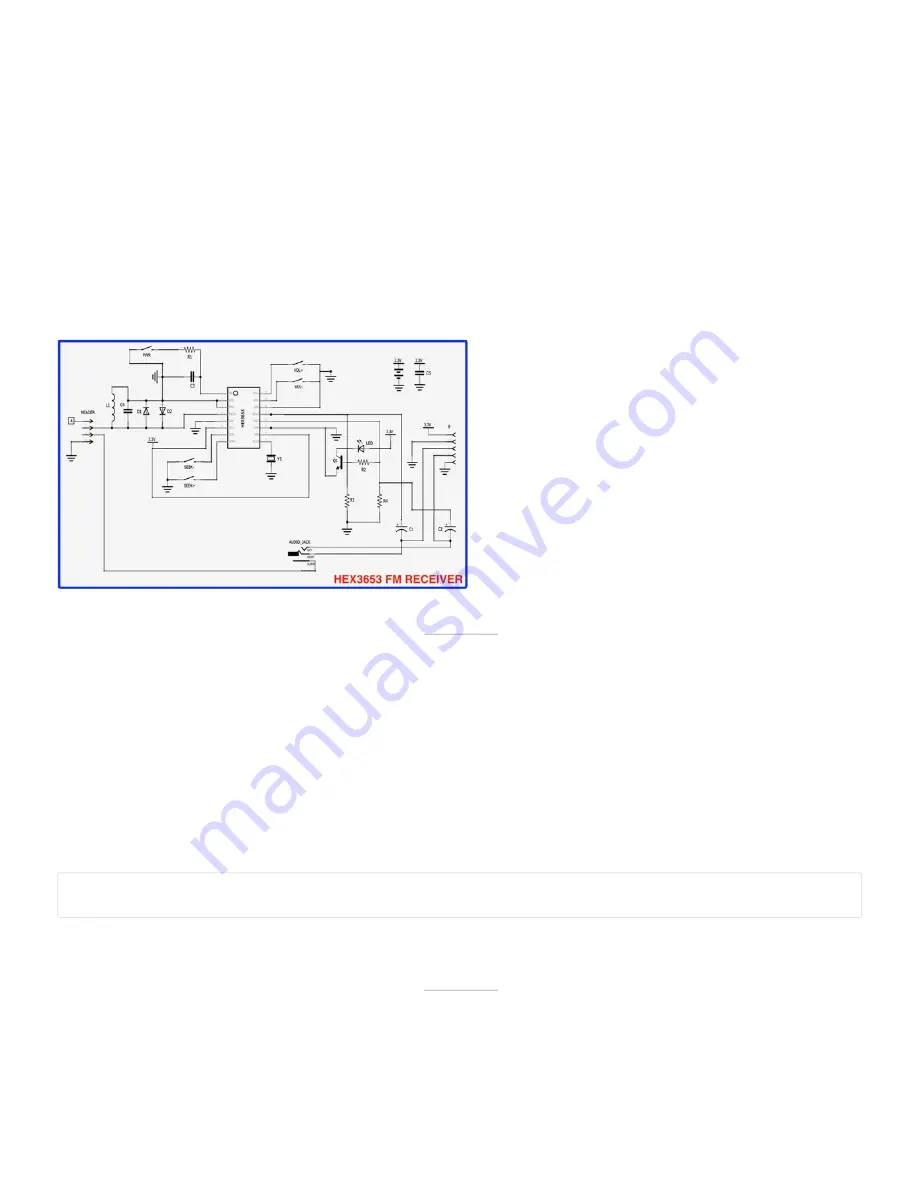
There are two options for an antenna input.
A wire can be attached to the "A" pad on the PCB or
the shielding of the headphone wire can serve as the
antenna.
The four-pin header serves as an antenna switch
(labeled ASW). Placement of the shorting jumper on
ASW selects between the two antenna inputs.
Shorting pins 1 and 2 routes the external antenna "A"
signal to pin four of the HEX3653 chip. Alternatively,
shorting pins 2 and 3 routes the shield pin of the
headphone jack to pin four of the HEX3653 chip.
Pin four of the HEX3653 chip is the radio frequency
(RF) input to the receiver chip. The selected RF signal
rst goes through L1 and C4 which act as a lter. Then
two clipping diodes are used to limit excessive input
voltage.
The ve-pin header (labeled B) allows the receiver
module to be integrated into another system. There
are two pins for power supply input (+V, ground) and
three for audio output (right, left, ground).
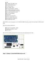
The three ceramic capacitors and the crystal and not
polarized and may be inserted in any orientation. They
are not interchangeable, but they may each be
rotated in their orientation. All of the other
components must be mounted according to the
orientation indicated on the PCB silkscreen. As usual,
it is best to start with the SMD chip, and then move to
the smallest/shortest components working from the
center of the PCB towards the edges. Attach the
headers, audio jack, and battery holder last.
https://youtu.be/-gX_-XVz3KI
HackerBox 0034: SubGHz: Page 9


