GOWIN GW1NR Series User Manual Download Page 20

3 View of Pin Distribution 

3.1 View of GW1NR-1 Pins Distribution 


UG119-1.5E 

13(34)


3


View of Pin Distribution 

3.1


View of GW1NR-1 Pins Distribution 

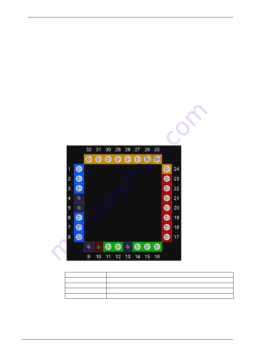
Figure 3-1 View of GW1NR-1 FN32G Pins Distribution (Top View) 


Table 3-1 Other pins in GW1NR-1 FN32G 

VCC 

VCCO0/VCCO1 

13 

VCCO2 

VCCO3 

VSS 

10 

Summary of Contents for GW1NR Series

Page 1: ...GW1NR series of FPGA products Package Pinout User Guide UG119 1 5E 02 02 2021 ...

Page 2: ...Office and other countries All other words and logos identified as trademarks or service marks are the property of their respective holders as described at www gowinsemi com cn GOWINSEMI assumes no liability provides no warranty either expressed or implied relating to the usage or intellectual property right infringement except as provided for by GOWINSEMI Terms and Conditions of Sale All informat...

Page 3: ...SRAM added 01 09 2019 1 08E QN88 of GW1NR4 embedded with PSRAM added View of pin distribution and I O bank description updated 07 09 2019 1 09E The GW1NR 9 MG100 package added 04 16 2020 1 1E GW1NR 9c added 05 18 2020 1 1 1E GW1NR 9 MG100PF added 06 12 2020 1 1 2E GW1NR 9C revised to GW1NR 9 06 30 2020 1 2E GW1NR 1 added 07 28 2020 1 3E GW1NR 9 MG100PD added 09 27 2020 1 4E GW1NR 9 MG100PA MG100PT...

Page 4: ...1NR 4 Pins 6 2 4 4 Quantity of GW1NR 9 Pins 8 2 5 Pin Definitions 8 2 6 Introduction to the I O BANK 12 3 View of Pin Distribution 13 3 1 View of GW1NR 1 Pins Distribution 13 3 2 View of GW1NR 2 Pins Distribution 14 3 2 1 View of MG49P Pins Distribution PSRAM Embedded 14 3 2 2 View of MG49PG Pins Distribution PSRAM and Flash Embedded 15 3 2 3 View of MG49G Pins Distribution Flash Embedded 16 3 3 V...

Page 5: ...bution 24 3 4 6 View of MG100PA Pins Distribution 25 3 4 7 View of MG100PS Pins Distribution 26 3 4 8 View of MG100PT Pins Distribution 27 4 Package Diagrams 28 4 1 QN88 QN88P Package Outline 10mm x 10mm 29 4 2 LQ144 LQ144P Package Outline 20mm x 20mm 30 4 3 MG49P MG49PG MG49G Package Outline 3 8mm x 3 8mm 31 4 4 MG81P Package Outline 4 5mm x 4 5mm 32 4 5 MG100P MG100PF MG100PA MG100PT MG100PS Pac...

Page 6: ...19 Figure 3 8 View of GW1NR 9 QN88 Pins Distribution Top View 20 Figure 3 9 View of GW1NR 9 QN88P Pins Distribution Top View 21 Figure 3 10 View of GW1NR 9 MG100P Pins Distribution Top View 22 Figure 3 11 View of GW1NR 9 MG100PF Pins Distribution Top View 23 Figure 3 12 View of GW1NR 9 LQ144P Pins Distribution Top View 24 Figure 3 13 View of GW1NR 9 MG100PA Pins Distribution Top View 25 Figure 3 1...

Page 7: ...W1NR 1 FN32G 13 Table 3 2 Other pins in GW1NR 2 MG49P PSRAM Embedded 14 Table 3 3 Other pins in GW1NR 2 MG49PG PSRAM and Flash Embedded 15 Table 3 4 Other pins in GW1NR 2 MG49G Flash Embedded 16 Table 3 5 Other pins in GW1NR 4 MG81P PSRAM Embedded 17 Table 3 6 Other pins in GW1NR 4 QN88P PSRAM Embedded 18 Table 3 7 Other pins in GW1NR 4 QN88 SDRAM Embedded 19 Table 3 8 Other pins in GW1NR 9 QN88 2...

Page 8: ...in numbers distribution of pins and package diagrams 1 2 Related Documents The latest user guidelines are available on the Gowin website at www gowinsemi com 1 DS117 GW1NR series of FPGA Products Data Sheet 2 UG290 Gowin FPGA Products Programming and Configuration User Guide 3 UG119 GW1NR series of FPGA Products Package and Pinout 4 UG805 GW1NR 2 Pinout 5 UG116 GW1NR 4 Pinout 6 UG803 GW1NR 9 Pinou...

Page 9: ...nchronous Dynamic RAM PSRAM Pseudo Static Random Access Memory GPIO Gowin Programmable IO QN88 QFN88 MG49P MBGA 49P MG49PG MBGA 49PG MG49G MBGA 49G MG81 MBGA81 MG100P MBGA100P MG100PF MBGA100PF MG100PA MBGA100PA MG100PT MBGA100PT MG100PS MBGA100PS LQ144 LQFP144 1 4 Support and Feedback Gowin Semiconductor provides customers with comprehensive technical support If you have any questions comments or...

Page 10: ...re in full compliance with the IPC 1752 standards 2 2 Package and Max User I O Information Table 2 1 Package and Max User I O Information LVDS Pairs Package Pitch mm Size mm GW1NR 1 GW1NR 2 GW1NR 4 GW1NR 9 FN32G 0 4 4 x 4 26 MG49P 0 5 3 8 x 3 8 30 8 MG49PG 0 5 3 8 x 3 8 30 8 MG49G 0 5 3 8 x 3 8 30 8 QN88 0 4 10 x 10 70 11 70 19 QN88P 0 4 10 x 10 70 11 70 18 MG81P 0 5 4 5 x 4 5 68 10 MG100P 0 5 5 x...

Page 11: ...I O plus one 2 3 Power Pin Table 2 2 Other Pins in the GW1NR Series VCC VCCO0 VCCO1 VCCO2 VCCO3 VCCX VSS NC 2 4 Pin Quantity 2 4 1 Quantity of GW1NR 1 Pins Table 2 3 Quantity of GW1NR 1 Pins Pin Type GW1NR 1 FN32G I O Single end Differential pair 1 BANK0 8 4 BANK1 5 2 BANK2 6 2 BANK3 8 3 Max User I O 2 27 Differential Pair 11 VCC 1 VCCO2 1 VCCO3 1 VCCO0 VCCO1 3 1 VSS 1 MODE0 0 MODE1 0 MODE2 0 JTAG...

Page 12: ...6 10 5 0 10 5 0 10 5 0 Max User I O 2 40 40 40 Differential Pair 20 20 20 True LVDS output 8 8 8 VCC 1 1 1 VCCX 1 1 1 VCCO0 1 1 1 VCCO1 1 1 1 VCCO2 VCCO3 V CCO4 VCCO5 3 1 1 1 VCCD 1 1 1 VCCOD 1 1 1 VSS 2 2 2 MODE0 0 0 0 MODE1 0 0 0 MODE2 0 0 0 JTAGSEL_N 0 0 0 Note 1 Quantity of single end differential LVDS I O include CLK pins and download pins 2 The JTAGSEL_N and JTAG pins cannot be used as I O s...

Page 13: ... GW1NR 4 Pins SDRAM embedded Pin Type GW1NR 4 QN88 I O Single end Differential pair 1 BANK0 18 5 0 BANK1 15 6 2 BANK2 23 9 7 BANK3 12 4 2 Max User I O 2 70 Differential Pair 24 True LVDS output 11 VCC 4 VCCX 0 VCCO0 0 VCCO1 1 VCCO2 2 VCCO3 1 VCCX VCCO0 3 3 VSS 6 MODE0 1 MODE1 1 MODE2 0 JTAGSEL_N 1 ...

Page 14: ...O 2 68 70 Differential Pair 21 24 True LVDS output 10 11 VCC 3 4 VCCX 1 0 VCCO0 1 0 VCCO1 1 1 VCCO2 1 2 VCCO3 1 1 VCCX VCCO0 3 0 3 VSS 4 6 MODE0 0 1 MODE1 1 1 MODE2 0 0 JTAGSEL_N 1 1 Note 1 Quantity of single end differential LVDS I O include CLK pins and download pins 2 The JTAGSEL_N and JTAG pins cannot be used as I O simultaneously The Max I O noted in this table is when the loaded four JTAG pi...

Page 15: ...LVDS output 19 18 20 16 16 17 17 17 VCC 4 4 4 3 3 3 3 3 VCCX 0 0 2 1 1 1 1 1 VCCO0 0 0 2 1 1 1 1 1 VCCO1 1 1 2 1 1 1 1 1 VCCO2 2 2 2 1 1 1 1 1 VCCO3 1 1 2 1 1 1 1 1 VCCX VCCO0 3 3 3 0 0 0 0 0 0 VSS 6 6 9 4 4 4 4 4 MODE0 1 1 1 0 0 0 0 0 MODE1 1 1 1 1 1 1 1 1 MODE2 0 0 0 0 0 0 0 0 JTAGSEL_N 1 1 1 1 1 1 1 1 Note 1 Quantity of single end differential LVDS I O include CLK pins and download pins 2 The J...

Page 16: ...de D3 I O Data port D3 in CPU mode D4 I O Data port D4 in CPU mode D5 I O Data port D5 in CPU mode D6 I O Data port D6 in CPU mode D7 I O Data port D7 in CPU mode RECONFIG_N I internal weak pull up Start new GowinCONFIG mode when low pulse READY I O When high level the device can be programmed and configured When low level the device cannot be programmed and configured DONE I O High level indicate...

Page 17: ...I L R PLL feedback input pin C Comp LPLL_T_in RPLL_T_in I L R PLL clock input pin T True LPLL_C_in RPLL_C_in I L R PLL clock input pin C Comp MODE2 I internal weak pull up GowinCONFIG modes selection pin if this pin is not bonded it s internal grounded MODE1 I internal weak pull up GowinCONFIG modes selection pin if this pin is not bonded it s internal grounded MODE0 I internal weak pull up GowinC...

Page 18: ...omparison input pin of data channel 3 for MIPI_DPHY_RX C Comp NC NA Reserved VSS NA Ground pins VCC NA Power supply pins for internal core logic VCCO NA Power supply pins for the I O voltage of I O BANK VCCX NA Power supply pins for auxiliary voltage Note 1 When the input is not single ended the GLKC_ x pin is not a global clock pin 2 DIO is a dedicated pin ...

Page 19: ... for further details Different IO Banks in the GW1NR series FPGA products are marked with different colors User I O power and ground are also marked with different symbols and colors The various symbols and colors used for the various pins are defined as follows denotes I Os in BANK0 denotes I Os in BANK1 denotes I Os in BANK2 denotes I Os in BANK3 denotes I Os in BANK4 denotes I Os in BANK5 denot...

Page 20: ...R 1 Pins Distribution UG119 1 5E 13 34 3View of Pin Distribution 3 1 View of GW1NR 1 Pins Distribution Figure 3 1 View of GW1NR 1 FN32G Pins Distribution Top View Table 3 1 Other pins in GW1NR 1 FN32G VCC 9 VCCO0 VCCO1 13 VCCO2 5 VCCO3 4 VSS 10 ...

Page 21: ... GW1NR 2 Pins Distribution 3 2 1 View of MG49P Pins Distribution PSRAM Embedded Figure 3 2 View of GW1NR 2 MG49P Pins Distribution Top View PSRAM Embedded Table 3 2 Other pins in GW1NR 2 MG49P PSRAM Embedded VCC C3 VCCD E4 VCCOD E5 VCCO0 C5 VCCO1 D5 VCCO2 VCCO3 V CCO4 VCCO5 D3 VCCX E3 VSS C4 D4 ...

Page 22: ...w of MG49PG Pins Distribution PSRAM and Flash Embedded Figure 3 3 View of GW1NR 2 MG49PG Pins Distribution Top View PSRAM and Flash Embedded Table 3 3 Other pins in GW1NR 2 MG49PG PSRAM and Flash Embedded VCC C3 VCCD E4 VCCOD E5 VCCO0 C5 VCCO1 D5 VCCO2 VCCO3 V CCO4 VCCO5 D3 VCCX E3 VSS C4 D4 ...

Page 23: ...E 16 34 3 2 3 View of MG49G Pins Distribution Flash Embedded Figure 3 4 View of GW1NR 2 MG49G Pins Distribution Top View Flash Embedded Table 3 4 Other pins in GW1NR 2 MG49G Flash Embedded VCC C3 VCCD E4 VCCOD E5 VCCO0 C5 VCCO1 D5 VCCO2 VCCO3 V CCO4 VCCO5 D3 VCCX E3 VSS C4 D4 ...

Page 24: ...View of GW1NR 4 Pins Distribution 3 3 1 View of MG81P Pins Distribution PSRAM Embedded Figure 3 5 View of GW1NR 4 MG81P Pins Distribution Top View PSRAM Embedded Table 3 5 Other pins in GW1NR 4 MG81P PSRAM Embedded VCC A2 A8 J2 VCCX J8 VCCO0 A5 VCCO1 E9 VCCO2 J5 VCCO3 E1 VSS A1 A9 J1 J9 ...

Page 25: ...5E 18 34 3 3 2 View of QN88P Pins Distribution PSRAM Embedded Figure 3 6 View of GW1NR 4 QN88P Pins Distribution Top View PSRAM Embedded Table 3 6 Other pins in GW1NR 4 QN88P PSRAM Embedded VCC 1 22 45 66 VCCX VCCO0 64 67 78 VCCO1 58 VCCO2 23 44 VCCO3 12 VSS 2 21 24 43 46 65 ...

Page 26: ... 5E 19 34 3 3 3 View of QN88 Pins Distribution SDRAM Embedded Figure 3 7 View of GW1NR 4 QN88 Pins Distribution Top View SDRAM Embedded Table 3 7 Other pins in GW1NR 4 QN88 SDRAM Embedded VCC 1 22 45 66 VCCX VCCO0 64 67 78 VCCO1 58 VCCO2 23 44 VCCO3 12 VSS 2 21 24 43 46 65 ...

Page 27: ...E 20 34 3 4 View of GW1NR 9 Pins Distribution 3 4 1 View of QN88 Pins Distribution Figure 3 8 View of GW1NR 9 QN88 Pins Distribution Top View Table 3 8 Other pins in GW1NR 9 QN88 VCC 1 22 45 66 VCCX VCCO0 64 67 78 VCCO1 58 VCCO2 23 44 VCCO3 12 MODE 87 88 VSS 2 21 24 43 46 65 ...

Page 28: ...ribution UG119 1 5E 21 34 3 4 2 View of QN88P Pins Distribution Figure 3 9 View of GW1NR 9 QN88P Pins Distribution Top View Table 3 9 Other pins in GW1NR 9 QN88P VCC 1 22 45 66 VCCX VCCO0 64 67 78 VCCO1 58 VCCO2 23 44 VCCO3 12 MODE 87 88 VSS 2 21 24 43 46 65 ...

Page 29: ... Distribution UG119 1 5E 22 34 3 4 3 View of MG100P Pins Distribution Figure 3 10 View of GW1NR 9 MG100P Pins Distribution Top View Table 3 10 Other pins in GW1NR 9 MG100P VCC A2 J2 A8 VCCO0 A5 VCCO1 E9 VCCO2 J5 VCCO3 E1 VCCX J8 MODE D4 VSS A1 A9 J1 J9 ...

Page 30: ...Distribution UG119 1 5E 23 34 3 4 4 View of MG100PF Pins Distribution Figure 3 11 View of GW1NR 9 MG100PF Pins Distribution Top View Table 3 11 Other pins in GW1NR 9 MG100PF VCC A2 J2 A8 VCCO0 A5 VCCO1 E9 VCCO2 J5 VCCO3 E1 VCCX J8 MODE D4 VSS A1 A9 J1 J9 ...

Page 31: ...1 5E 24 34 3 4 5 View of LQ144P Pins Distribution Figure 3 12 View of GW1NR 9 LQ144P Pins Distribution Top View Table 3 12 Other pins in GW1NR 9 LQ144P VCC 1 36 73 108 VCCO0 109 127 VCCO1 91 103 VCCO2 37 55 VCCO3 9 19 VCCX 31 77 MODE 143 144 VSS 2 17 33 35 53 74 89 105 107 ...

Page 32: ...Distribution UG119 1 5E 25 34 3 4 6 View of MG100PA Pins Distribution Figure 3 13 View of GW1NR 9 MG100PA Pins Distribution Top View Table 3 13 Other pins in GW1NR 9 MG100PA VCC A2 J2 A8 VCCO0 A5 VCCO1 E9 VCCO2 J5 VCCO3 E1 VCCX J8 MODE D4 VSS A1 A9 J1 J9 ...

Page 33: ...Distribution UG119 1 5E 26 34 3 4 7 View of MG100PS Pins Distribution Figure 3 14 View of GW1NR 9 MG100PS Pins Distribution Top View Table 3 14 Other pins in GW1NR 9 MG100PS VCC A2 A8 J2 VCCO0 A5 VCCO1 E9 VCCO2 J5 VCCO3 E1 VCCX J8 MODE D4 VSS A1 A9 J1 J9 ...

Page 34: ...Distribution UG119 1 5E 27 34 3 4 8 View of MG100PT Pins Distribution Figure 3 15 View of GW1NR 9 MG100PT Pins Distribution Top View Table 3 15 Other pins in GW1NR 9 MG100PT VCC A2 A8 J2 VCCO0 A5 VCCO1 E9 VCCO2 J5 VCCO3 E1 VCCX J8 MODE D4 VSS A1 A9 J1 J9 ...

Page 35: ...4 Package Diagrams UG119 1 5E 28 34 4Package Diagrams ...

Page 36: ...TOM VIEW SYMBOL A1 c D D2 e Nd E E2 Ne L MAX MILLIMETER MIN NOM 0 75 0 70 0 80 0 02 0 0 05 0 20 0 15 0 25 0 20 0 18 0 25 6 74 6 64 6 84 10 00 9 90 10 10 0 40 0 30 0 50 0 40BSC 8 40REF E2 Nd Ne L PIN 1 Laser Mark 1 88 22 23 44 45 66 67 EXPOSED PAD ZONE h h 8 40REF 6 74 6 64 6 84 K K 0 20 h 0 35 0 30 0 40 D2 SIDE VIEW TOP VIEW L F载体尺寸 mil 300x300 1 2 88 A 0 85 0 80 0 90 b1 0 10REF b1 0 90 0 85 0 95 ...

Page 37: ...4 Package Diagrams 4 2 LQ144 LQ144P Package Outline 20mm x 20mm UG119 1 5E 30 34 4 2 LQ144 LQ144P Package Outline 20mm x 20mm Figure 4 2 Package Outline LQ144 LQ144P ...

Page 38: ...4 Package Diagrams 4 3 MG49P MG49PG MG49G Package Outline 3 8mm x 3 8mm UG119 1 5E 31 34 4 3 MG49P MG49PG MG49G Package Outline 3 8mm x 3 8mm Figure 4 3 Package Outline MG49P MG49PG MG49G ...

Page 39: ...4 Package Diagrams 4 4 MG81P Package Outline 4 5mm x 4 5mm UG119 1 5E 32 34 4 4 MG81P Package Outline 4 5mm x 4 5mm Figure 4 4 Package Outline MG81P ...

Page 40: ... MG100P MG100PF MG100PA MG100PT MG100PS Package Outline 5mm x 5mm UG119 1 5E 33 34 4 5 MG100P MG100PF MG100PA MG100PT MG100PS Package Outline 5mm x 5mm Figure 4 5 Package Outline MG100P MG100PF MG100PA MG100PT E D E1 D1 100X ...

Page 41: ...4 Package Diagrams 4 6 FN32G Package Outline 4mm x 4mm UG119 1 5E 34 34 4 6 FN32G Package Outline 4mm x 4mm Figure 4 6 Package Outline FN32G ...

Page 42: ......

Reviews: