background image

1-7-1

E1T12FW

FIRMWARE RENEWAL MODE

Note:

The file extension of the available firmware is 
“b30”. 

1.

Turn the power on and remove the disc on the tray 
and close the tray.

2.

To put the BD player into version up mode, press 
[9], [8], [7], [6], and [POP MENU/MENU] buttons 
on the remote control unit in that order. The tray 
will open automatically. 
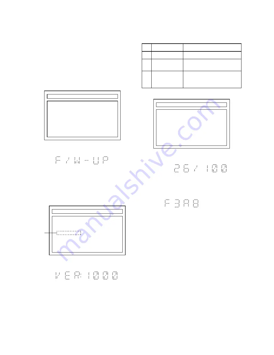
Fig. a appears on the screen and Fig. b appears 
on the VFD.

Fig. a  Version Up Mode Screen

Fig. b  VFD in Version Up Mode

3.

Load the disc for version up.

4.

The BD player enters the F/W version up mode 
automatically. Fig. c appears on the screen and 
Fig. d appears on the VFD. Make sure to insert the 
proper F/W for the state of this model. 

Fig. c  Programming Mode Screen (Example)

Fig. d  VFD in Programming Mode (Example)

The appearance shown in (*1) of Fig. c is described as 

follows:

Fig. e  Version Up Mode

Fig. f  VFD in Version Up Mode

5.

After programming is finished, the checksum on 
the VFD (Fig. g).

Fig. g  VFD upon Finishing the Programming Mode (Example)

Checksum appears on the VFD then the tray will open 

automatically. Remove the disc on the tray.

At this time, no button is available.

6.

Unplug the AC cord from the AC outlet. Then plug 
it again.

7.

Turn the power on.

Note:

All the settings will be put back to factory-
default.

"*******" differ depending on the models.

F/W VERSION UP MODE

F/W Name:*******  Ver *.***

Please Insert a Disc
        For F/W Version Up

"*******" differ depending on the models.

F/W VERSION UP MODE

F/W Name:*******  Ver *.***

EXIT : POWER

Now Loading...

(*1)

No.

Appearance

State

1

Now Loading... Loading the disc

2

Reading...

Sending files into the 
memory. 

3

See FL Display.

Writing new version data,
the progress will be displayed 
as shown in Fig. f.

"*******" differ depending on the models.

F/W VERSION UP MODE

F/W Name:*******  Ver *.***

EXIT : POWER

1. ALL

Version : *.***                  **************.b30
CHECKSUM : ****

See FL Display.

Summary of Contents for HT2-M200

Page 1: ...2ED HT2 M200 E1T13ED model For the HT2 M200 E1T12ED HT2 M200 E1T13ED model the letter E1T12ED E1T13ED is printed on the Rating Label on the back of the unit Refer to the Rating Label below Rating Labe...

Page 2: ...ray Disc Home Theater 1 6 1 Firmware Renewal Mode 1 7 1 Troubleshooting 1 8 1 Internet Radio vTuner Error Code 1 9 1 Block Diagrams 1 10 1 Schematic Diagrams and CBA 1 11 1 Waveforms 1 12 1 Wiring Dia...

Page 3: ...1 1 1 E1T12SP SPECIFICATIONS...

Page 4: ...ay from the pickup lens when the diode is turned on Do not look directly at the laser beam CAUTION Use of controls and adjustments or doing procedures other than those specified herein may result in h...

Page 5: ...fied B In addition to safety other parts and assemblies are specified for conformance with regulations applying to spurious radiation These must also be replaced only with specified replacements Examp...

Page 6: ...parts RF terminals antenna terminals video and audio input and output terminals microphone jacks earphone jacks etc is lower than or equal to the specified value in the table below Measuring Method Po...

Page 7: ...chine then apply hot air to the Flat Pack IC about 5 to 6 seconds Fig S 1 1 2 Remove the flat pack IC with tweezers while applying the hot air 3 Bottom of the flat pack IC is fixed with glue to the CB...

Page 8: ...y one using a sharp pin or wire to which solder will not adhere iron wire When heating the pins use a fine tip soldering iron or a hot air desoldering machine Fig S 1 4 3 Bottom of the flat pack IC is...

Page 9: ...ig S 1 6 Note When using a soldering iron care must be taken to ensure that the flat pack IC is not being held by glue When the flat pack IC is removed from the CBA handle it gently because it may be...

Page 10: ...ed to remove any static electricity that may be charged on the body 2 Ground for Workbench Be sure to place a conductive sheet or copper plate with proper grounding 1 M on the workbench or other surfa...

Page 11: ...BA BD Mechanism Assembly is adjusted as a unit at factory Therefore do not disassemble it Replace the BD Main CBA BD Mechanism Assembly as a unit 3 When reassembling be sure to use the original screws...

Page 12: ...CBA 4 Front CBA S 3 S 3 CN3002 S 2 5 Front Assembly Fig D3 6 BD Main CBA BD Mechanism Assembly CN404 CN6101 CN7001 S 4 S 6 S 5 S 5 Locking Card Spacer M PCB Plate Earth See Reference Note 2 Fig D4 7 F...

Page 13: ...1 5 3 E1T12DC 9 AV CBA 10 AMP PSU CBA CN402 CN403 PCB Bracket Front CN9002 S 12 S 13 S 13 Fig D6 11 SD Card CBA 12 MP3 CBA S 14 S 15 Fig D7...

Page 14: ...cord and then plug it in 2 Turn the power on by pressing the OPEN CLOSE button and the disc tray will open automatically Procedure B 1 Remove the Top Cover Front Assembly BD Main CBA BD Mechanism Asse...

Page 15: ...ons on the remote control unit in that order Fig a appears on the screen All VFD lights Fig a 4 Press C button on the remote control unit Fig b appears on the screen and Fig c appears on the VFD Fig b...

Page 16: ...ig c is described as follows Fig e Version Up Mode Fig f VFD in Version Up Mode 5 After programming is finished the checksum on the VFD Fig g Fig g VFD upon Finishing the Programming Mode Example Chec...

Page 17: ...the tray and close the tray 3 Press 1 2 3 4 and DISPLAY buttons on the remote control unit in that order Fig h appears on the screen All VFD lights Fig h 4 To exit this mode press button differ depend...

Page 18: ...d as shown in Fig i on the VFD Fig h Fig i VFD in Update Mode 8 GOODBYE on the VFD and power turns off automatically when it finishes 9 The power turns on and the tray will open automatically Remove t...

Page 19: ...EMBLY if defective Yes FLOW CHART NO 2 The fuse blows out After servicing replace the fuse F9000 Check the presence that the primary component is leaking or shorted and replace AMP PSU CBA if defectiv...

Page 20: ...RT NO 4 Audio does not appear normally Set the disc on the disc tray and playback Yes Are the audio signals serial data outputted to Pin 3 4 5 6 of CN201 Replace BD Main CBA BD MECHANISM ASSEMBLY Repl...

Page 21: ...re shown in the list below The Detailed Error Code shows the three digit code used in the HTTP Status Code or used internally in the Application The HTTP Status Codes 200 to 500 series are defined in...

Page 22: ...an invalid reply from another proxy or the original server 503 Service Unavailable Because of overloading or maintenance the server is temporarily unavailable Status Code Description 001 Nothing List...

Page 23: ...d to unit s connection request 743 System Error Program A system error occurred in the unit program error internal cURL processing error 745 System Error LAN Port A system error occurred in the unit L...

Page 24: ...TU_SDA TU_SCL SCL SDA W_SDA W_SCL SW SDOUT2 4 W_TSD1 3 W_SCLK W_SCLK MCLK XL201 8MHz CN204 5pin CN205 7pin debug1 5 EV 3V3 3 3V UART5_TX UART5_RX upgate_SW FAN Control AD FAN_LOCK CEC SAFETY CEC IN CE...

Page 25: ...replacement parts that do not have the same safety characteristics as specified in the parts list may create shock fire or other hazards Notes 1 Do not use the part number shown on these drawings for...

Page 26: ...upply Otherwise it may cause some components in the power supply circuit to fail 3 Note 1 Do not use the part number shown on the drawings for ordering The correct part number is shown in the parts li...

Page 27: ...2 XTALI 3 XTALO 4 MCLKI 5 MICLK_DIV 6 CS0 7 GPIO 8 DVDD 9 DVSS 10 SDIN1 11 SDIN2 12 SDIN3 13 SDIN4 14 SDA1 15 SCL1 16 SDA2 17 SCL2 18 LRCLK 19 SCLKIN 20 MCLKO 21 SCLKOUT1 22 SCLKOUT2 23 SDOUT4 24 SDOU...

Page 28: ...3A C9054 104P U5V 5V 1 5V 2 D9017 open D9015 1N4148 D9016 1N4148 C9153 open C9152 470U 10V C9151 470U 10V R9035 10K BK3V3 Safety C9142 104P 100V 1 2 3 4 5 6 7 8 9 10 11 12 13 14 15 16 17 18 19 20 21 2...

Page 29: ...B JRC4558 IN 12V IN 12V FB306 600 OHM C439 0 1UF C438 100UF AV 5V_2 AV 5V S 6 VCC 5 Y 4 I0 3 GND 2 I1 1 IC306 Open S 6 VCC 5 Y 4 I0 3 GND 2 I1 1 IC307 Open VIGND VIGND IPOD 5V VCC 1 DET 2 RX 3 GND 4 R...

Page 30: ...9 P10 P11 P12 P13 P14 P15 P16 P17 P18 FL5001 MATRIX CHART S7 S8 S2 S4 S3 h h h h h h h S5 S6 S1 S9 f j a f j a f j a f j a f f f j j j S10 S11 S12 S13 g s k b m e r p n c d g s k b m e r p n c d g s k...

Page 31: ...VSSQ E7 VSSQ F2 VSSQ F8 VSSQ H2 VSSQ H8 VSSDL J7 CK J8 CK K8 CKE K2 NC A2 NC E2 BA2 L1 NC R3 NC R7 NC R8 IC6501 K4T1G164QQ HCE7 BA0 L2 BA1 L3 A12 R2 A11 P7 A10 AP M2 A9 P3 A8 P8 A7 P2 A6 N7 A5 N3 A4...

Page 32: ...CK74A C20 VC27A D20 AEXCKA T34 XRST AC30 XSRST R6714 10K 1005 R6008 56 1005 R6009 56 1005 R6701 10K 1005 DGND R6012 2 2K 1005 R6062 10K 1005 R6063 10K 1005 R6067 10K 1005 R6066 10K 1005 R6061 10K 100...

Page 33: ...35 82 1005 C7511 47P C7512 47P C7513 47P C7514 47P C7515 47P DGND PON 3V3_BE C7550 47P C7551 47P C7552 47P C7553 47P L7511 OPEN 2125 L7513 OPEN 2125 L7514 OPEN 2125 L7512 OPEN 2125 C7554 47P L7501 R S...

Page 34: ...CN7601 BM05B SRSS TB LF SN 1 5V 2 DN 3 DP 4 GND 5 FG C7022 0 1 F 1005 R7601 0 1608 R7101 82 F R7103 82 F R7105 82 F R7107 82 F VG VG VG AG R7630 0 1608 PON 3V3_BE AUDIO 5V BD2224G IC7601 VIN GND EN O...

Page 35: ...AL1 VDDIO AL12 VDDIO AL15 VDDIO AL18 VDDIO AL2 VDDIO AL6 VDDIO AM11 VDDIO AM5 VDDIO AA6 VDDIOCK AF6 VDDIOCK AJ14 VDDIOCK B1 VDD33 C2 VDD33 D3 VDD33 E4 VDD33 F11 VDD33 F15 VDD33 F20 VDD33 F23 VDD33 F5...

Page 36: ...R6440 49 9 F 1608 R6439 49 9 F 1608 R6446 33K 1005 D6401 SML 310VTT86K D6402 SML 310VTT86K IC6401 KSZ8041TL 1 GND 2 GND 3 GND 4 VDDA_1 8 5 VDDA_1 8 6 V1 8_OUT 7 VDDA_3 3 8 VDDA_3 3 9 RX 10 RX 11 TX 1...

Page 37: ...32 CTL_MTR B25 FG B24 P37 PS C21 NEJECT TSM A20 P33 F34 LDDSAVE M30 LDDENA A22 PWM5B E22 PWM6B F28 LPC2 C29 LPC1 F27 LPCO2 E27 LPC3 C28 LPCO1 D27 LPCO3 TP349 CTL_MTR TP348 PS R362 10K TP201 AIN TP202...

Page 38: ...PWM INT_WSPK TP7013 TP7014 R7038 0 1005 R7039 0 1005 AO2__DATA2_ADAC AO2_MCLK_ADAC SBO 3 SBT 3 AO2_LRCK_ADAC AIN_L PWM_MUTE AO2__DATA3_ADAC SB3_PIO AIN_PDN AIN_R AO2__DATA0_ADAC AO2_BCK_ADAC AIN_SCLK...

Page 39: ...2 0 1 F C7303 10 2125 C7301 0 01 F C7304 0 1 F C7305 0 1 F C7306 0 1 F DGND C7307 0 01 F C7310 0 1 F C7308 0 1 F C7309 10 2125 C7311 0 01 F C7312 0 01 F C7313 0 1 F C7314 0 1 F C7315 0 1 F C7316 0 1 F...

Page 40: ...AC power supply Otherwise it may cause some components in the power supply circuit to fail NOTE The voltage for parts in hot circuit is measured using hot GND as a common terminal Because a hot chass...

Page 41: ...ise it may cause some components in the power supply circuit to fail NOTE The voltage for parts in hot circuit is measured using hot GND as a common terminal AMP PSU CBA Bottom View Because a hot chas...

Page 42: ...1 11 18 AV CBA Top View...

Page 43: ...1 11 19 PIN 29 OF CN404 WF3 PIN 27 OF CN404 WF2 PIN 25 OF CN404 WF1 PIN 23 OF CN404 WF4 AV CBA Bottom View...

Page 44: ...P3004 TP3005 TP3006 TP3008 TP3007 TP3009 TP3010 TP3011 TP3012 TP3013 CN3001 CN3002 C3001 C3002 C3003 C3004 C3005 Q3001 C3006 C3007 C3008 C3009 C3010 C3011 C3012 C3013 C3014 C3015 SW3001 SW3002 SW3003...

Page 45: ...1 11 21 MP3 CBA Bottom View MP3 CBA Top View SD Card CBA Top View SD Card CBA Bottom View...

Page 46: ...050 R6052 C312 C313 R6053 TP6110 C314 R6630 R6055 C315 TP6111 R6631 C316 R6632 C317 R6633 C7213 R6634 R6635 R6442 R357 R6443 R358 R359 C7601 TP402 C7602 C7603 C514 C7605 C7606 C7607 TP213 TP407 C324 C...

Page 47: ...R7576 R7577 R7578 R7579 R107 R109 C6414 R7580 R301 C6415 R7581 R302 C6416 C6417 R7584 C6418 IC6001 C6419 R7585 R306 R7586 R113 R7587 R114 R115 R7589 R116 R117 R118 R119 R501 R6012 R502 R6013 R503 R50...

Page 48: ...Pin 23 of CN404 Component Component Cb Cb 0 2V 0 2V 20 20 sec sec Component Component Cr Cr 0 2V 0 2V 20 20 sec sec WF2 Pin 27 of CN404 Component Y Component Y 0 2V 0 2V 20 20 sec sec CVBS CVBS 0 5V 0...

Page 49: ...IF OUT 18 19 DGND 19 20 SPDIF IN 20 21 DGND 21 22 VOGND 22 23 CVBS OUT 23 24 VOGND 24 25 Component Y OUT 25 26 VOGND 26 27 Component Cb OUT 27 28 VOGND 28 29 Component Cr OUT 29 30 VOGND 30 CN6101 CN9...

Page 50: ...07 2L002 B1 2L022 2L021 B20 2L023 2L024 A6 A2 A6 2L031 2L030 2L030 B16 2L030 AX1 A21 A20 A22 Front CBA AV CBA AMP PSU CBA Power SW CBA BD Main CBA BD Mechanism Assembly SD Card CBA MP3 CBA 2L005 2L008...

Page 51: ...1 14 2 E1T12_13PEX Packing S2 X3 X6 X20 A X7 X5 X2 S3 S1 B X10 S1 A X1 A21 Some Ref Numbers are not in sequence A30 X20 B X20 C X20 D X21 X23 X22 HT2 M200 E1T12ED...

Page 52: ...VM412937A 2L022 SCREW C TIGHT M3X6 E5610UD 0VM412937A 2L023 SCREW C TIGHT M3X6 E5610UD 0VM412937A 2L024 SCREW C TIGHT M3X6 E5610UD 0VM412937A 2L030 SCREW P TIGHT M3X8 BIND HEAD GBJP3080 2L031 SCREW P...

Page 53: ...C CAP 100 F 10V M H7 or CEB101ENW025 CAP ELECTROLYTIC 100 F 10V M H7 or CA1A101ENE10 ELECTROLYTIC CAP 100 F 10V M H7 CE1AMAVSL101 CONNECTORS CN3001 FPC FFC CONNECTOR 25P IMSA 9615S 25C PP A JC96J25ER0...

Page 54: ...QSAB or SST0101AL038 TACT SWITCH KSM0612B SST0101HH003 SW3002 TACT SWITCH SKQSAB or SST0101AL038 TACT SWITCH KSM0612B SST0101HH003 SW3003 TACT SWITCH SKQSAB or SST0101AL038 TACT SWITCH KSM0612B SST010...

Page 55: ...HT2 M200 E1T12ED 13ED 2010 09 24...

Reviews: