262
CHAPTER 16 8/16-BIT PPG
16.4
Operations of 8/16-bit PPG
One 8/16-bit PPG consists of two channels of 8-bit PPG units. These two channels can
be used in three modes: independent two-channel mode, 8-bit pre 8-bit PPG
mode, and single-channel 16-bit PPG mode.
■
Operations of 8/16-bit PPG
Each of the 8-bit PPG units has two eight-bit reload registers. One reload register is for the "L" pulse width
(PRLL) and the other is for the "H" pulse width (PRLH). The values stored in these registers are reloaded
into the 8-bit down counter (PCNT), from the PRLL and PRLH in turn. The pin output value is inverted
upon a reload caused by counter borrow. This operation results in the pulses of the specified "L" pulse
width and "H" pulse width.
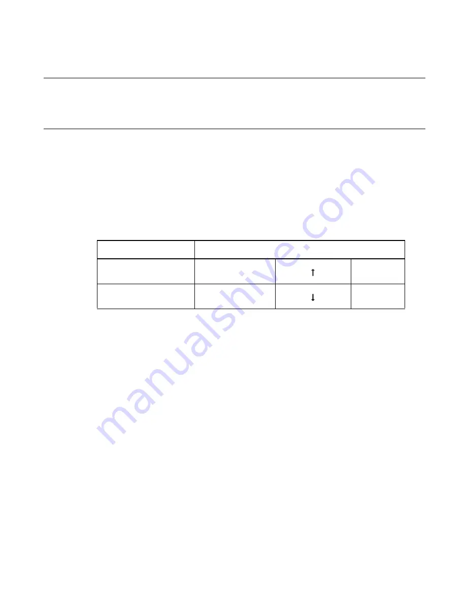
Table 16.4-1 lists the relationship between the reload operation and pulse outputs.
When "1" is set in bit4 (PIE0) of PPGC0 or in bit12 (PIE1) of PPGC1, an interrupt request is output upon a
borrow from "00
H
" to "FF
H
" (from "0000
H
" to "FFFF
H
" in 16-bit PPG mode) of each counter.
■
Operation Modes of 8/16-bit PPG
This block can be used in three modes: independent two-channel mode, 8-bit pre 8-bit PPG mode,
and single-channel 16-bit PPG mode.
●
Independent two-channel mode
The two channels of 8-bit PPG units operate independently. The PPG00 pin is connected to the ch.0 PPG
output, while the PPG10 pin is connected to the ch.1 PPG output.
●
8-bit pre 8-bit PPG mode
Ch.0 is used as an 8-bit prescaler while the count in ch.1 is based on borrow outputs from ch.0. Thus, 8-bit
PPG waveforms can be output with arbitrary length of cycle time. The PPG00 pin is connected to the ch.0
prescaler output, while the PPG10 pin is connected to the ch.1 PPG output.
●
16-bit PPG 1ch mode
Ch.0 and ch.1 are connected and used as a single 16-bit PPG. The PPG00 and PPG10 pins are connected to
the 16-bit PPG output.
Table 16.4-1 Reload Operation and Pulse Output
Reload operation
Pin output change
PRLH
→
PCNT
PPG0/PPG1 [0
→
1]
Rise
PRLL
→
PCNT
PPG0/PPG1 [1
→
0]
Fall
Summary of Contents for MB90390 Series
Page 2: ......
Page 4: ......
Page 17: ...xiii APPENDIX D List of Interrupt Vectors 690 INDEX 695 ...
Page 18: ...xiv ...
Page 132: ...104 CHAPTER 5 CLOCKS ...
Page 152: ...124 CHAPTER 6 CLOCK MODULATOR ...
Page 210: ...182 CHAPTER 11 TIME BASE TIMER ...
Page 218: ...190 CHAPTER 12 WATCHDOG TIMER ...
Page 264: ...236 CHAPTER 14 16 BIT RELOAD TIMER WITH EVENT COUNT FUNCTION ...
Page 274: ...246 CHAPTER 15 WATCH TIMER ...
Page 306: ...278 CHAPTER 17 DTP EXTERNAL INTERRUPTS ...
Page 338: ...310 CHAPTER 18 8 10 BIT A D CONVERTER ...
Page 364: ...336 CHAPTER 19 UART0 UART1 ...
Page 398: ...370 CHAPTER 20 UART2 UART3 Figure 20 5 2 ORE Set Timing Receive data RDRF ORE ...
Page 432: ...404 CHAPTER 20 UART2 UART3 ...
Page 482: ...454 CHAPTER 22 SERIAL I O ...
Page 560: ...532 CHAPTER 24 STEPPING MOTOR CONTROLLER ...
Page 582: ...554 CHAPTER 27 ROM MIRRORING MODULE ...
Page 632: ...604 CHAPTER 29 EXAMPLES OF SERIAL PROGRAMMING CONNECTION ...
Page 722: ...694 APPENDIX ...
Page 723: ...695 INDEX The index follows on the next page This is listed in alphabetic order ...
Page 740: ......


