


MB39A104
4
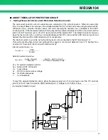
■
BLOCK DIAGRAM
+
+
++
+
+
+
+
+
+
+
+
10
VREF
VREF
11
9
6
15
14
16
19
8
CS1
FB1
DTC1
CS2
FB2
DTC2
CSCP
12 13
18
17
RT CT
GND
VREF
24
7
23
2
20
21
22
5
4
3
1
CTL
VCC
GNDO
VH
ILIM2
VS2
OUT2
ILIM1
VS1
OUT1
VCCO
1.24 V
1.24 V
(3.1 V)
SCP
Comp.
SCP
Logic
UVLO
OSC
VREF
Bias
Voltage
Current
Protection
Logic
Current
Protection
Logic
I
O
=
200 mA
at VCCO
=
12 V
I
O
=
200 mA
at VCCO
=
12 V
VR1
VH
1.24 V
2.5 V
1.5 V
5.0 V
bias
Power
ON/OFF
CTL
P-ch
Drive2
P-ch
Drive1
PWM
Comp.1
PWM
Comp.2
Error
Amp2
Error
Amp1
CH1
CH2
−
INE1
−
INE2
10
µ
A
V
CC
−
5 V
10
µ
A
L priority
L priority
L priority
L priority
H priority
H: at SCP
H:UVLO
release
Accuracy
±
1%
H: at OCP
Error Amp Power Supply
Error Amp Referennce
Summary of Contents for MB39A104
Page 38: ...MB39A104 38 MEMO ...
Page 39: ...MB39A104 39 MEMO ...


