


MPC563XM Reference Manual, Rev. 1
Freescale Semiconductor
731
Preliminary—Subject to Change Without Notice
tooth transition indications in Angle Mode. Further details can be found on
and
Section 23.4.7, “EAC - eTPU Angle Counter
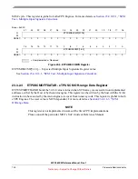
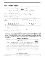
Like the channel input signals, the TCRCLK signal has an associated synchronizer followed by a digital
filter. This digital filter can work in two sub-modes, whose purpose is to filter out noise pulses that have
width less then a programmed value of system clocks, preventing these transitions from being input to the
transition detect logic. The synchronizer and digital filter are guaranteed to pass pulses that are greater than
a programmed value. The clock and operation sub-mode of the TCRCLK filter is configured
independently of the other channel input filters, through the field TCRCF in register ETPUTBCR. For
more information on filter sub-modes, refer to
Section 23.4.6.5, “TCRCLK Digital Filter
Angle Modes, the output of the digital filter of channel 0 is replaced with the output of TCRCLK signal
digital filter (see
Section 23.4.7, “EAC - eTPU Angle Counter
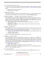
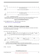
23.2.2.4
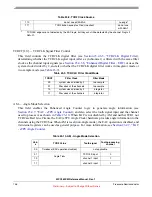
ipp_ind_etpu_odis_[1|2]([0-3]) eTPU Channel Output Disable Signals
Each of these 4 input signals are used to force the outputs of a group of 8 channels to an inactive level.
When an ODIS input is active, all the channels in its group of 8 that have their bits ODIS=1 in ETPUCxCR
register have their outputs forced to the opposite of the value specified in bit OPOL of the same register.
Therefore, channels can be individually selected to be affected by the output disable signals, as well as
their disabling forced polarity (see
The output disable channel groups are defined in
In a Dual-engine eTPU there are 8 output disable signals for the 64 channels.
23.3
Memory Map/Register Definition
The guideline for the description of all bits and fields throughout
Section 23.3, “Memory Map/Register
” is to provide only a brief explanation (without examples or method of use) of the features,
since it will be used mainly as a reference for the reader that is studying
, where those features are explained in detail.
23.3.1
Memory Map
The eTPU System simplified memory map is shown in
. Each of the register areas shown may
have their own reserved address areas.
shows a detailed memory map. Offsets are relative to the eTPU Base address, which is
MCU-dependent.
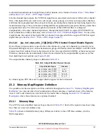
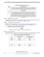
Table 23-2. Output Disable Channel Groups
Output Disable Signal
Channels
ipp_ind_etpu_odis_[1!2](0)
0 to 7
ipp_ind_etpu_odis_[1|2](1)
8 to 15
ipp_ind_etpu_odis_[1|2](2)
16 to 23
ipp_ind_etpu_odis_[1|2](3)
24 to 31


