


MPC563XM Reference Manual, Rev. 1
1222
Freescale Semiconductor
Preliminary—Subject to Change Without Notice
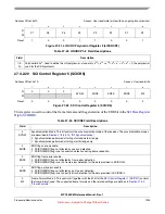
27.3.2.6
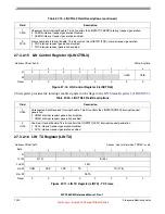
SCI Control Register 4 (SCICR4)
This register provides the interrupt enable bits for the interrupt flags provided in
and control bits for the transmitter and receiver.
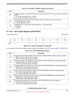
Table 27-10. SCICR3 Field Descriptions
Field
Description
7
MDIS
Module Disabled Mode. This bit controls the Module Mode of Operation, which is described in
”
0 Module is not in Disabled Mode.
1 Module is in Disabled Mode.
6
FBR
Fast Bit Error Detection. This bit controls the Bit Error Detection mode.
0 Standard Bit error detection performed as described in
Section 27.4.6.5.3, “Standard Bit Error Detection
”.
1 Fast Bit error detection performed as described in
Section 27.4.6.5.4, “Fast Bit Error Detection
Note:
This bit is used in LIN mode only.
5
BSTP
Bit Error or Physical Bus Error Stop. This bit controls the transmit DMA requests generation in case of bit errors
or physical bus errors. Bit errors are indicated by the BERR flag in the
SCI Status Register 2 (SCISR2)
physical bus errors are indicated by the PBERR flag in the
LIN Status Register 1 (LINSTAT1)
0 Transmit DMA requests generated regardless of bit errors or physical bus errors.
1 Transmit DMA requests are
not
generated if SCISR2[BERR] flag or LINSTAT1[PBERR] flag are set.
Note:
This bit is used in LIN mode only.
4
BERRIE
Bit Error Interrupt Enable. This bit controls the BERR interrupt request generation.
0 BERR interrupt request generation disabled.
1 BERR interrupt request generation enabled.
3
RXDMA
Receive DMA Control. This bit enables the receive DMA feature.
0 Receive DMA disabled.
1 Receive DMA enabled.
2
TXDMA
Transmit DMA Control. This bit enables the transmit DMA feature.
0 Transmit DMA disabled.
1 Transmit DMA enabled.
1
BRCL
Break Character Length. This bit is used to define the length of the break character to be transmitted.
The settings are specified in
Section 27.4.2.2, “Break Character Formats
”.
0
TXDIR
TXD pin output enable. This bit determines whether the TXD pin is used as an output.
0 TXD pin is not used as output.
1 TXD pin is used as output.
Note:
This bit is used in Single Wire Mode only.
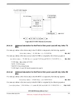
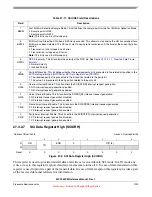
Address Offset: 0x5
Access: User read/write
7
6
5
4
3
2
1
0
R
BESM
BESTP
RXPOL
PMSK
ORIE
NFIE
FEIE
PFIE
W
Reset
0
0
0
0
0
0
0
0
Figure 27-7. SCI Control Register 4 (SCICR4)


