


MPC563XM Reference Manual, Rev. 1
1108
Freescale Semiconductor
Preliminary—Subject to Change Without Notice
3. Since the expected values for the conversion of these voltages are known (CAL_RES
25%VREF
and
CAL_RES
75%VREF
), GCC and OCC values can be calculated from equations <st-plain> and
<st-plain> using these values, and the ones determined in steps 1 and 2.
4. Reformat GCC and OCC to the proper data formats as specified in the
section. GCC is an unsigned 15-bit fixed point value and OCC is a
signed 14-bit value.
Section 24.5.3.4, “ADC0/1 Gain Calibration Constant Registers
and OCC value to
Section 24.5.3.5, “ADC0/1 Offset
Calibration Constant Registers (ADC0_OCCR and ADC1_OCCR)
commands.
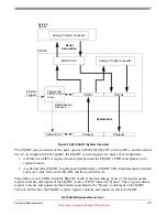
24.7.6.2
Example
The raw results obtained when sampling reference voltages 25%VREF and 75%VREF were, respectively,
3798 and 11592. The results that should have been obtained from the conversion of these reference
voltages are, respectively, 4096 and 12288. Therefore, using equations <st-plain> and <st-plain>, the gain
and offset calibration constants are:
GCC=(12288-4096)/(11592-3798) = 1.05106492-> 1.05102539 = 0x4388
OCC=12288 - 1.05106492*11592 - 2 = 102.06-> 102 = 0x0066
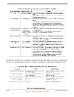
shows, for this particular case, examples of how the result values change according to GCC
and OCC when result calibration is executed (CAL=1) and when it is not (CAL=0).
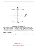
24.7.6.3
Quantization Error Reduction During Calibration
shows how the ADC transfer curve changes due to the addition of two to the MAC output
during the calibration - see MAC output equation at
absolute quantization error is reduced by half leading to an increase in accuracy.
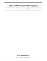
Table 24-41. Calibration example
Input Voltage
Raw result (CAL=0)
Calibrated result (CAL=1)
Hexadecimal
Decimal
Hexadecimal
Decimal
25% VREF
0x0ED6
3798
0x1000
4095.794
75% VREF
0x2D48
11592
0x3000
12287.486


