


ELECTRICAL CHARACTERISTICS
MC68332
A-22
USER’S MANUAL
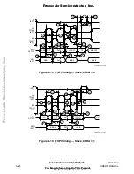
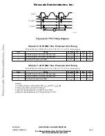
NOTES:
1. All AC timing is shown with respect to 20% V
DD
and 70% V
DD
levels unless otherwise noted.
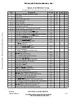
Table A-7 Background Debugging Mode Timing
(V
DD
= 5.0 Vdc
±
10%, V
SS
= 0 Vdc, T
A
= T
L
to T
H
)
Num
Characteristic
Symbol
Min
Max
Unit
B0
DSI Input Setup Time
t
DSISU
15
—
ns
B1
DSI Input Hold Time
t
DSIH
10
—
ns
B2
DSCLK Setup Time
t
DSCSU
15
—
ns
B3
DSCLK Hold Time
t
DSCH
10
—
ns
B4
DSO Delay Time
t
DSOD
—
25
ns
B5
DSCLK Cycle Time
t
DSCCYC
2 —
t
cyc
B6
CLKOUT High to FREEZE Asserted/Negated
t
FRZAN
—
50
ns
B7
CLKOUT High to IFETCH High Impedance
t
IFZ
—
50
ns
B8
CLKOUT High to IFETCH Valid
t
IF
—
50
ns
B9
DSCLK Low Time
t
DSCLO
1
—
t
cyc
B10
FREEZE Asserted to IFETCH Valid
t
FRZIF
TBD
—
t
cyc
F
re
e
sc
a
le
S
e
m
ic
o
n
d
u
c
to
r,
I
Freescale Semiconductor, Inc.
For More Information On This Product,
Go to: www.freescale.com
n
c
.
..


