5
3 Signal Description
3.1 Signal Diagram
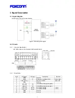
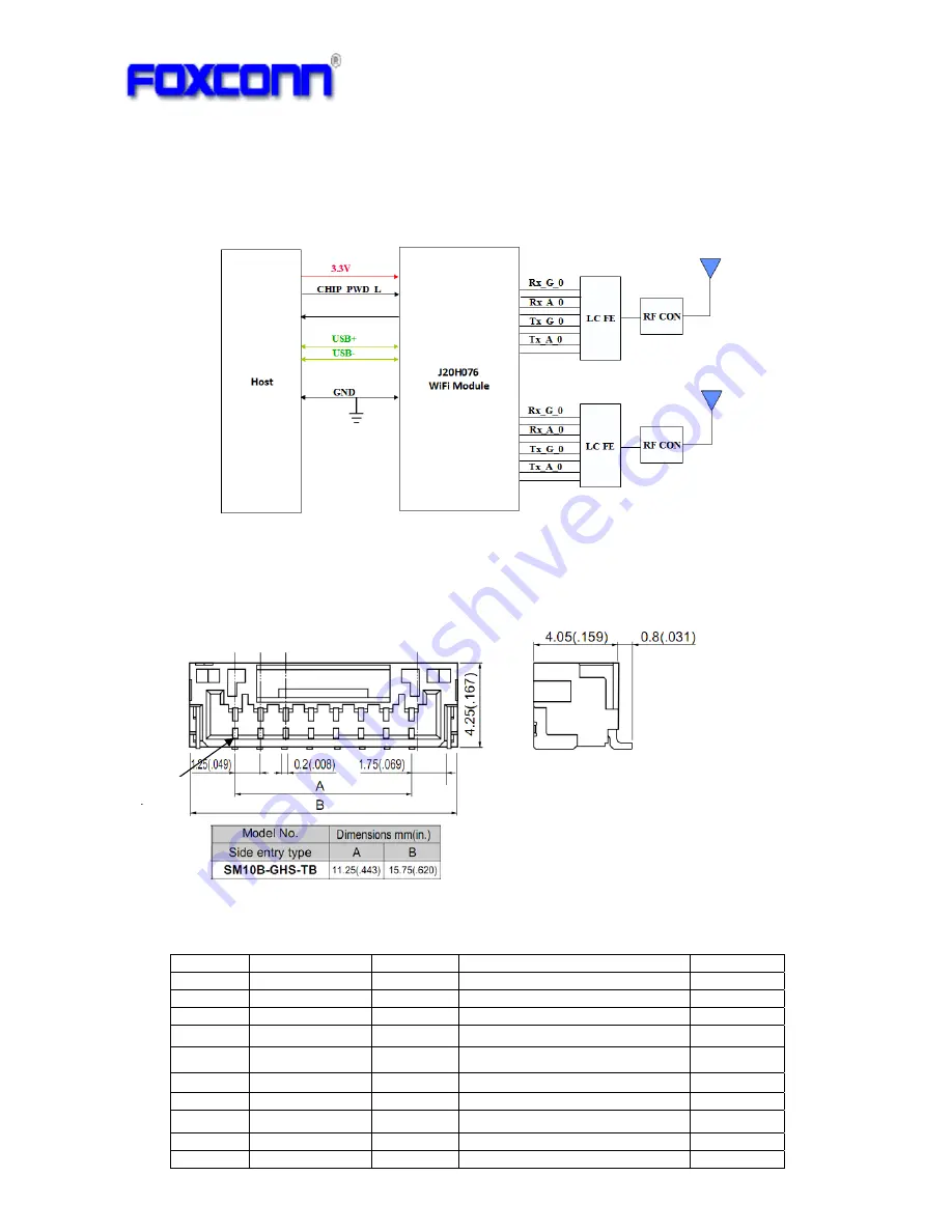
Below figure 2 shows its signal diagram.
Figure 2: Module Signal Diagram
3.2 Pinouts
3.2.1 Connector
Specification
JST WTB connector, Part Number: SM10B-GHS-TB(LF)
3.2.2 Pin
definition
Pin#
Pin Name
Pin Type
Description
Remark
1 GND -
Ground
2
WoW
O
Wake-up on wireless LAN
Active high
3
CHIP_PWD_L
I
Reset to module
Active low
4 GND -
Ground
5 USB_DM I/O
USB differential signal negative
6 USB_DP I/O
USB differential signal positive
7
VCC_3.3V
Power
3.3V power supply
+/-5%
8 VCC_3.3V
Power
3.3V power supply
+/-5%
9 GND -
Ground
10 GND -
Ground
Pin1
Summary of Contents for QCA9375
Page 3: ...3 1 Revision History Date Document revision Change History 2013 5 24 1 0 Initial release...
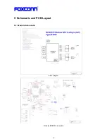
Page 13: ...13 5 Schematic and PCB Layout 5 1 Module Schematic Block Diagram Mckinley BB MAC Transceiver...
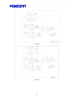
Page 14: ...14 RF Chain 0 RF Chain 1...
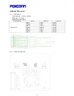
Page 16: ...16 5 2 3 PCB Layout Layer 1 TOP View Layer 2 TOP View...
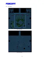
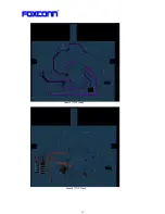
Page 17: ...17 Layer 3 TOP View Layer 4 TOP View...
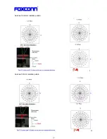
Page 19: ...19 Antenna 0 2 4GHz radiation pattern Antenna 0 5GHz radiation pattern...
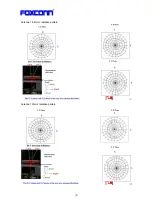
Page 20: ...20 Antenna 1 2 4GHz radiation pattern Antenna 1 5GHz radiation pattern...
Page 21: ...21 7 Module Mechanical Specifications Dimension W x L x H 40 0mmx37 5mmx5 45mm...
Page 23: ...23 9 Reliability Test Plan...
Page 24: ...24...
Page 26: ...26 11 Packing Information...
Page 27: ...27...

