background image


1.


Level


1


Environment

related


Substances


should


NEVER


be


used.


2.


Purchase


ink,


paint,


wire


rods,


and


molding


resins


only


from


the


business


partners


that


Sony


approves


as


Green


Partners.


3.


Recycled


Resin


and


Coated


Wire


should


be


procured


from


Green


Partners


User


Manual


IEEE


802.11a/b/g/n


2x2


WiFi


Module


Project


Name


QCA9375


IEEE


802.11a/b/g/n


2x2


WiFi


Module


Customer


Part


No.


021430401


Approval


Sheet


Rev.


1.0


Foxconn


Part


No.


J20H076.01


Prepared


by


Reviewed


by


Approved


by


Gallon


G.R.


Tao


Robin


Xu


Chang

Fu


Lin


HON HAI PRECISION IND. CO., LTD. 
No.2, 2nd Dong Huan Road, 10th 
YouSong lndustrial District, Longhua 
Town, Baoan, ShenZhen 

Summary of Contents for QCA9375

Page 1: ...Wire should be procured from Green Partners User Manual IEEE 802 11a b g n 2x2 WiFi Module Project Name QCA9375 IEEE 802 11a b g n 2x2 WiFi Module Customer Part No 021430401 Approval Sheet Rev 1 0 Fox...

Page 2: ...cification 802 11g 8 4 5 3 WLAN RF Specification 802 11n 2 4GHz HT20 9 4 5 4 WLAN RF Specification 802 11a 10 4 5 5 WLAN RF Specification 802 11n 5GHz HT20 11 4 5 6 WLAN RF Specification 802 11n 5GHz...

Page 3: ...3 1 Revision History Date Document revision Change History 2013 5 24 1 0 Initial release...

Page 4: ...5MHz 5845MHz 1 2 Modulation DBPSK DQPSK CCK BPSK QPSK 16QAM 64QAM 1 3 Data Rates 1 2 5 5 11Mbps 11b 6 9 12 18 24 36 48 54 Mbps 11g MCS0 MCS15 1 4 Security it supports WEP TKIP AES WPA WPA2 and WAPI 1...

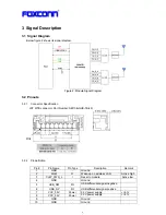
Page 5: ...M10B GHS TB LF 3 2 2 Pin definition Pin Pin Name Pin Type Description Remark 1 GND Ground 2 WoW O Wake up on wireless LAN Active high 3 CHIP_PWD_L I Reset to module Active low 4 GND Ground 5 USB_DM I...

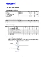
Page 6: ...0 3 3 3 3 46 V 4 3 Power Consumption Symbol Condition Min Typ Max Unit Supply voltage 3 0 3 3 3 6 V Tx Current 1Mbps 16dBm MIMO 465 mA Tx Current 11g 54Mbps 14 5dBm MIMO 400 mA Tx Current 11gn MCS15...

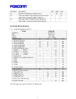
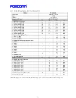
Page 7: ...7 5 dBm 2 Target Power 2Mbps 14 5 16 a 17 5 dBm 3 Target Power 5 5Mbps 14 5 16 a 17 5 dBm 4 Target Power 11Mbps 14 5 16 a 17 5 dBm 2 Spectrum Mask Target Power 1 fc 33MHz f fc 22MHz 50 dBr 2 fc 22MHz...

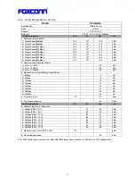
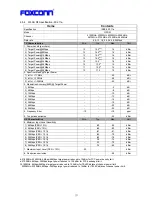
Page 8: ...m Mask Target Power 1 at fc 11MHz 20 dBr 2 at fc 20MHz 28 dBr 3 at fc 30MHz 40 dBr 3 Modulation Accuracy EVM Target Power 1 6Mbps 5 dB 2 9Mbps 8 dB 3 12Mbps 10 dB 4 18Mbps 13 dB 5 24Mbps 16 dB 6 36Mbp...

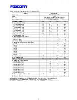
Page 9: ...get Power MCS5 12 5 14 c 15 5 dBm 7 Target Power MCS6 12 5 14 c 15 5 dBm 8 Target Power MCS7 11 5 13c 14 5 dBm 2 Spectrum Mask Target Power 1 at fc 11MHz 20 dBr 2 at fc 20MHz 28 dBr 3 at fc 30MHz 45 d...

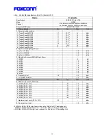
Page 10: ...acy EVM Target Power 1 6Mbps 5 dB 2 9Mbps 8 dB 3 12Mbps 10 dB 4 18Mbps 13 dB 5 24Mbps 16 dB 6 36Mbps 19 dB 7 48Mbps 22 dB 8 54Mbps 25 dB 4 Frequency Error 10 10 ppm 5 Tx spurious emission 52 dBm RX Ch...

Page 11: ...2 12 13 5 g h i 15 dBm 4 Target Power MCS3 12 13 5 g h i 15 dBm 5 Target Power MCS4 12 13 5 g h i 15 dBm 6 Target Power MCS5 11 12 5 g i 14 dBm 7 Target Power MCS6 10 11 5 13 dBm 8 Target Power MCS7 9...

Page 12: ...4 dBm 4 Target Power MCS3 11 12 5 j k 14 dBm 5 Target Power MCS4 11 12 5 j k 14 dBm 6 Target Power MCS5 10 11 5 j k 13 dBm 7 Target Power MCS6 9 10 5 j 12 dBm 8 Target Power MCS7 8 9 5 11 dBm 2 Spectr...

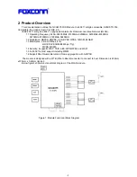
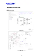
Page 13: ...13 5 Schematic and PCB Layout 5 1 Module Schematic Block Diagram Mckinley BB MAC Transceiver...

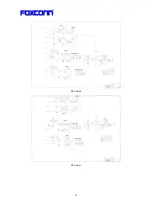
Page 14: ...14 RF Chain 0 RF Chain 1...

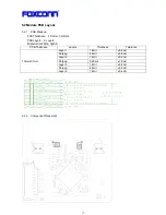
Page 15: ...B Layers 4 Layers Material HF FR4 Tg150 PCB Thickness Layers Thickness Tolerance Layer 1 1 8mil 0 4mil Perpeg 4 5mil 0 5mil Layer 2 1 2mil 0 2mil Perpeg 24 0mil 1 9mil Layer 3 1 2mil 0 2mil Perpeg 4 5...

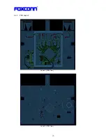
Page 16: ...16 5 2 3 PCB Layout Layer 1 TOP View Layer 2 TOP View...

Page 17: ...17 Layer 3 TOP View Layer 4 TOP View...

Page 18: ...ntenna Specifications 6 1 PCB Printed Antenna Pattern Ant 0 and Ant 1 pattern are horizontal mirror Ant 0 Ant 1 6 2 Antenna Radiation Performance Antenna VSWR and Isolation Antenna Peak gain and Effic...

Page 19: ...19 Antenna 0 2 4GHz radiation pattern Antenna 0 5GHz radiation pattern...

Page 20: ...20 Antenna 1 2 4GHz radiation pattern Antenna 1 5GHz radiation pattern...

Page 21: ...21 7 Module Mechanical Specifications Dimension W x L x H 40 0mmx37 5mmx5 45mm...

Page 22: ...e Condition 1 Moisture barrier bag must be stored under 40 humidity under 90 RH when the moisture barrier bag is sealed by Foxconn 2 The calculated shelf life for the dry packed product shall be a 12...

Page 23: ...23 9 Reliability Test Plan...

Page 24: ...24...

Page 25: ...he laser marking details 1 2D barcode content is total 37 digits include MAC ID Customer data and SONY Part Number 2 MAC address 3 Foxconn model name Label version 4 Foxconn manufacture order 5 SONY P...

Page 26: ...26 11 Packing Information...

Page 27: ...27...

Reviews: