background image

Reproduction forbidden without Fibocom Wireless Inc. written authorization - All Rights Reserved

FIBOCOM L610-LA Series Hardware Guide

Page 45 of

49

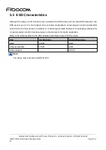
5.5 ESD Characteristics

Although the design of L610 module has considered the ESD issues and provided ESD protection, the
ESD issue may occur in the transport and secondary development, so developers should consider ESD
protection for the final product. In addition to considering anti-static treatment for packaging, please refer
to recommended circuit for interface design in the document for client’s application.
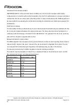
Refer to the following table for the ESD allowable discharge range of L610 module.

Part

Air Discharge

Contact Discharge

GND

±15KV

±8KV

Antenna interface

±15KV

±8KV

Other interface

-

±0.5KV

Note:

The above data is tested on ADP-L610-00.

Summary of Contents for L610-LA

Page 1: ...Draft FIBOCOM L610 LA Hardware Guide Version V1 1 1 Date 2020 05 29...

Page 2: ...dden without Fibocom Wireless Inc written authorization All Rights Reserved FIBOCOM L610 LA Series Hardware Guide Page 2 of 49 Applicability type No Product model Description 1 L610 LA MAIN_ANT FDD TD...

Page 3: ...ividual is prohibited to excerpt copy any part of or the entire document or transmit the document in any form Notice The document is subject to update from time to time owing to the product version up...

Page 4: ...ower domain V1 0 3 Wang Yuanguang Wang Bo Liu Ke 2019 12 17 Modified module thickness issue V1 0 4 Wang Yuanguang Wang Bo Liu Ke 2019 12 31 Added power consumption data V1 0 5 Wang Yuanguang Wang Bo L...

Page 5: ...on Interface 12 3 1 LCC LGA Interface 12 3 1 1 Pin Distribution 12 3 1 2 Pin Definition 13 3 1 3 Pin Multiplexing 21 3 2 Power Supply 22 3 2 1 Power Supply 22 3 2 2 1 8V Output 23 3 2 3 Power Consumpt...

Page 6: ...1 NET_MODE Signal 35 3 8 Low Power Consumption Mode 37 3 8 1 Flight Mode 37 3 8 2 Sleep Mode 37 3 9 ADC Function 37 4 RF Interface 38 4 1 L610 Operating Band 38 4 2 L610 RF Output Power 38 4 3 L610 RF...

Page 7: ...you drive do not use the handheld devices even if it has a hand free feature Please stop and call Please turn off the mobile device before boarding The wireless feature of the mobile device is not all...

Page 8: ...k Radio transmission and reception TDD 3GPP TS 36 521 1 V10 6 0 User Equipment UE conformance specification Radio transmission and reception Part 1 Conformance testing 3GPP TS 21 111 V10 0 0 USIM and...

Page 9: ...FDD Band 1 2 3 4 5 7 8 28 66 LTE TDD NO Support GSM 850 900 1800 1900 ANT Main WIFI Built in ESIM NO Support 2 2 Product Specifications Specifications Operating band LTE FDD Band 1 2 3 4 5 7 8 28 66...

Page 10: ...update USB Voice service AMR caller ID call forwarding call hold call waiting and multi party call etc SMS service Point to point MO MT cell broadcast Text and PDU modes Note When the normal operating...

Page 11: ...Reproduction forbidden without Fibocom Wireless Inc written authorization All Rights Reserved FIBOCOM L610 LA Series Hardware Guide Page 11 of 49 Figure 2 2 Hardware diagram...

Page 12: ...re Guide Page 12 of 49 3 Application Interface 3 1 LCC LGA Interface L610 modules adopt LCC 80PIN LGA 64PIN packaging with a total of 144 pins 3 1 1 Pin Distribution Figure 3 1 Pin Distribution Diagra...

Page 13: ...6V VIHmin 1 2V VIHmax 2 0V L SLEEP_IND Left floating when not in use 4 W_DISABLE I VILmin 0 3V VILmax 0 63V VIHmin 1 2 2 2V VIHmax 2 0 2 8V L Module flight mode control Left floating when not in use...

Page 14: ...1 35V For 3 0V USIM VILmax 1 0V VIHmin 1 95V VOLmax 0 45V VOHmin 2 55V USIM data signal cable 16 USIM_CLK O For 1 8V USIM VOLmax 0 45V VOHmin 1 35V For3 0V USIM VOLmax 0 45V VOHmin 2 55V USIM clock si...

Page 15: ...g when not in use 28 SDC2_DATA_3 I O VILmin 0 3V VILmax 0 63V VIHmin 1 2 2 2V VIHmax 2 0 2 8V H SDC2_DATA_3 Left floating when not in use 29 SDC2_DATA_2 I O VILmin 0 3V VILmax 0 63V VIHmin 1 2 2 2V VI...

Page 16: ...Lmin 0 3V VILmax 0 6V VIHmin 1 2V VIHmax 2 0V L SPI_MISO Left floating when not in use 40 SPI_CLK O VOLmax 0 45V VOHmin 1 35V VILmin 0 3V VILmax 0 6V VIHmin 1 2V VIHmax 2 0V L SPI_CLK Left floating wh...

Page 17: ...55 NC NC 56 GND G Ground 57 VBAT_RF PI Vmax 4 2V Vmin 3 4V Vnorm 3 8V RF power input 3 4V 4 2V 58 VBAT_RF PI Vmax 4 2V Vmin 3 4V Vnorm 3 8V RF power input 3 4V 4 2V 59 VBAT_BB PI Vmax 4 2 Vmin 3 4V V...

Page 18: ...ting when not in use 68 RXD I VILmin 0 3V VILmax 0 6V VIHmin 1 2V VIHmax 2 0V Module Receive data Left floating when not in use 69 USB_DP I O USB signal DP Left floating when not in use 70 USB_DM I O...

Page 19: ...I KEYOUT3 Left floating when not in use 115 USB_BOOT I USB_BOOT Enter DL mode before upgrading 116 NC NC 117 CLK26M_OUT O CLK26M_OUT Left floating when not in use 118 NC NC 119 LCD_FMARK O VILmin 0 3V...

Page 20: ...V VIHmax 2 0V L PM_EN_WLAN Left floating when not in use 128 NC NC 129 SD1_DATA3 I O VILmin 0 3V VILmax 0 6V VIHmin 1 2V VIHmax 2 0V L SD1_DATA3 Left floating when not in use 130 SD1_DATA2 I O VILmin...

Page 21: ...n 1 2V VIHmax 2 0V L BT_EN Left floating when not in use 140 NC NC 141 I2C2_SCL I O VILmin 0 3V VILmax 0 6V VIHmin 1 2V VIHmax 2 0V L I2C2_SCL Left floating when not in use 142 I2C2_SDA I O VILmin 0 3...

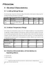
Page 22: ...3 8V VDD_EXT O 7 Voltage output 1 8V GND 8 9 19 22 36 46 48 50 54 56 85 112 Ground 3 2 1 Power Supply L610 modules need to be powered by the VBAT pin The recommended power design is shown in Figure 3...

Page 23: ...imum operating current can reach 2A and the power voltage needs to be at least 3 3V Otherwise the module may power off or restart The power limit is shown in Figure 3 3 Figure 3 3 Power Limit Note Cli...

Page 24: ...80 GPRS Data transfer DCS1800 PCL 0 1Rx 4Tx 400 GPRS Data transfer PCS1900 PCL 0 1Rx 4Tx 400 ILTE RMS LTE FDD LTE FDD Data transfer Band 1 23dBm 730 LTE FDD Data transfer Band 2 23dBm 780 LTE FDD Data...

Page 25: ...3 1 Module Power on 3 3 1 1 Power on Circuit Reference When L610 module is in powered off mode the module will power on by pulling down PWRKEY for at least 2s It is recommended to use OC OD drive cir...

Page 26: ...rol Diagram Note Before pulling down the PWRKEY pin make sure that the VBAT voltage is stable It is recommended that the interval between power up VBAT and pull down PWRKEY pin should not be less than...

Page 27: ...e shutdown Pull down PWRKEY for at least 3 1s and then release Normal shutdown AT shutdown AT CPWROFF Software shutdown 1 When the module is working properly do not cut off the power of the module imm...

Page 28: ...28 of 49 3 3 3 1 Reset Circuit The reset reference circuit is shown in Figure 3 6 It is similar to the PWRKEY control circuit The client can control the RESET_N pin using an OC OD drive circuit or bu...

Page 29: ...e of PCB to avoid module reset caused by ESD 3 4 USB Interface L610 modules support USB 2 0 and are compatible with USB High Speed 480Mbits s and USB Full Speed 12Mbits s Refer to Universal Serial Bus...

Page 30: ...al lines shall be parallel and equal in length and shall avoid right angle wiring USB_DM and USB_DP signal cables are routed on the signal layer closest to the ground layer and the lines shall be wrap...

Page 31: ...re Guide Page 31 of 49 Figure 3 9 SIM Card Slot Diagram SIM016 8P 220P Figure 3 10 Reference Design of L610 USIM SIM Interface with Detection Signal Principles of SIM card slot with detection signal a...

Page 32: ...by detecting the USIM_ PRESENCE pin state of SIM card slot to support SIM hot plug function SIM hot plug function can be configured by AT MSMPD command and the AT commands are shown in the following...

Page 33: ...k signal cables and other strong interference sources Adopt the SIM card slot with metal shield shell to improve anti interference ability The length of cable from the module to the SIM card slot shal...

Page 34: ...odule Receive data The following table describes UART3 pin Pin Name I O Pin Description UART3_RXD I 137 Module Receive data UART3_TXD O 138 Module Transmit data The following table describes the debug...

Page 35: ...wn in the figure below The input and output circuit design in the following dashed part can refer to that in the solid line part but pay attention to the connection direction Figure 3 18 UART Signal C...

Page 36: ...ved L610 module network indicator NET_MODE status description Mode NET_MODE Description 1 Flash 600ms High 600ms Low No SIM SIM PIN Registering network T 15S Network registration failed 2 Slow flash 7...

Page 37: ...enter the flight mode 2 AT command control AT CFUN 4 enter the flight mode AT CFUN 1 enter the normal mode 3 8 2 Sleep Mode For details of sleep mode refer to FIBOCOM L610 AT Commands 3 9 ADC Function...

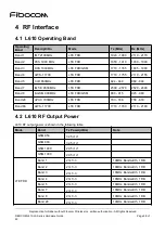
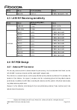
Page 38: ...69 894 Band 7 IMT E 2600MHz LTE FDD 2500 2570 2620 2690 Band 8 E GSM 900MHz LTE FDD GSM 880 915 925 960 Band 28 APAC 700MHz LTE FDD 703 748 758 803 Band 66 AWS 1 1700 LTE FDD 1710 1780 2110 2180 4 2 L...

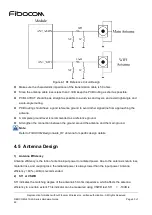
Page 39: ...d width Band 28 98 5 10MHz Band width Band 66 97 0 10MHz Band width 4 4 RF PCB Design 4 4 1 Antenna RF Connector The two way antenna of L610 module adopts the pad out way It is recommended that client...

Page 40: ...ignal line from approaching the antenna A complete ground level is recommended as a reference ground Strengthen the connection between the ground around the antenna and the main ground Note Refer to F...

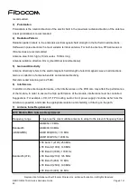
Page 41: ...of electromagnetic wave in all directions Gain is a collection of antenna benefits and antenna directivity Recommended antenna gain 2 5dBi 6 Interference In addition to the antenna performance other...

Page 42: ...All Rights Reserved FIBOCOM L610 LA Series Hardware Guide Page 42 of 49 L610 Module Main Antenna Requirements LTE Band 28 2100 100 MHz LTE Band 66 2100 100 MHz Impedance 50 ohms Input power 33dBm 2 W...

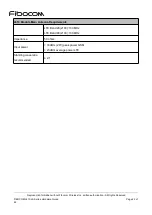
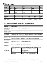
Page 43: ...perature Range L610 modules are recommended to operate at 30 75 ambient temperature It is recommended that the application considers temperature control measures in harsh environmental conditions At t...

Page 44: ...perature storage test Temperature 90 3 24 hours in shutdown state Temperature shock test In shutdown state 0 5 hour at 40 and 85 ambient temperatures respectively the temperature conversion time 3min...

Page 45: ...e transport and secondary development so developers should consider ESD protection for the final product In addition to considering anti static treatment for packaging please refer to recommended circ...

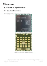
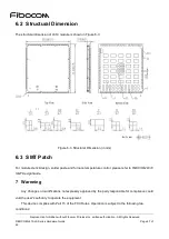
Page 46: ...All Rights Reserved FIBOCOM L610 LA Series Hardware Guide Page 46 of 49 6 Structure Specification 6 1 Product Appearance The product appearance of L610 module is shown in the figure below Figure 6 1...

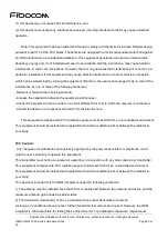
Page 47: ...Figure 6 3 Structural Dimension in mm 6 3 SMT Patch For module stencil design solder paste and furnace temperature control please refer to FIBOCOM L610 SMT Design Guide 7 Warnning Any Changes or modi...

Page 48: ...nd receiver Connect the equipment into an outlet on a circuit different from that to which the receiver is connected Consult the dealer or an experienced radio TV technician for help This equipment co...

Page 49: ...that 20 cm may be maintained between the antenna and users The final end product must be labeled in a visible area with the following Contains FCC ID ZMOL610LA The grantee s FCC ID can be used only wh...

Reviews: