background image

FSD200

8

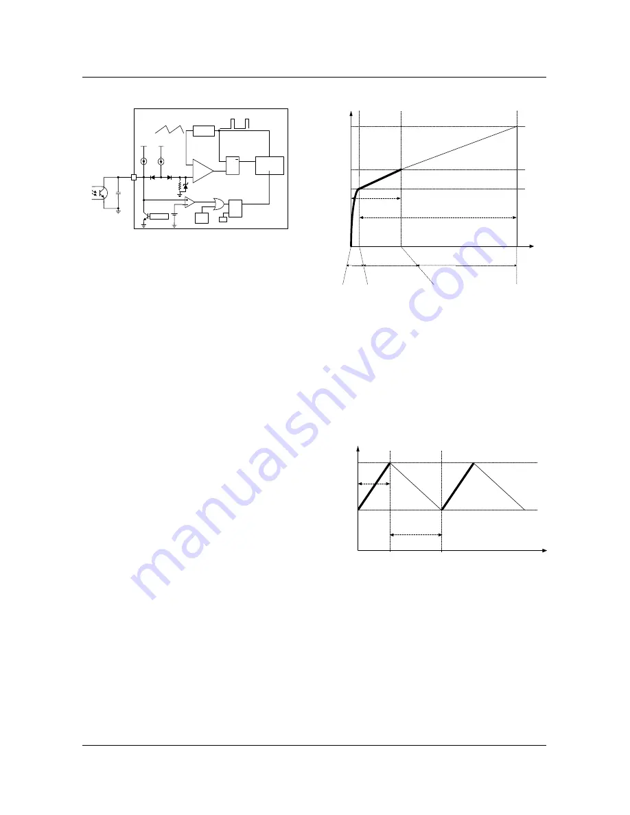
Figure 4. Protection block

4.1 Over Load Protection (OLP) : 

Overload is a load 

current that exceeds a pre-set level due to an abnormal 
situation. If this occurs, the protection circuit should be 
triggered to protect the SMPS. It is possible that a short 
term load transient can occur under normal operation. If 
this occurs the system should not shut down. In order 
to avoid false shut-downs, the over load protection 
circuit is designed to trigger after a delay. Therefore the 
device can discriminate between transient overloads 
and true faul conditions. The device is pulse-by-pulse 
current limited and therefore, for a given input voltage, 
the maximum input power is limited. If the load tries to 
draw more than this, the output voltage will drop below 
its set value. This reduces the opto-coupler LED 
current which in turn will reduce the photo-transistor
current. Therefore, the 250uA current source will 
charge the feedback pin capacitor, Cfb, and the 
feedback voltage, Vfb, will increase. The input to the 
feedback comparator is clamped at around 3V. 
Therefore, once Vfb reaches 3V, the device is 
switching at maximum power. At this point the 250uA 
current source is blocked and the 5uA source continues 
to charge Cfb. Once Vfb reaches 4V, switching stops. 
Therefore the shutdown delay time is set by the time 
required to charge Cfb from 3V to 4V with 5uA as 
shown in Fig. 5.

Figure 5. Over load protection delay

4.2 Thermal Shutdown (TSD) :

 The SenseFET and 

the control IC are assembled in one package. This 
makes it easy for the control IC to detect the 
temperature of the SenseFET. When the temperature
exceeds approximately 150

°

C, thermal shutdown is

activated. Thermal shutdown has a Hysteresis of 50

°

and so the temperature must drop to 100

°

C before the 

device attempts to restart. 

5. Soft Start

 : FSD200/210 has an internal soft start 

circuit that increases the feedback voltage together 
with the MOSFET current slowly at start up. The soft 
start time is 3msec in FSD200/210.

OSC

4

Vfb

S

R

Q

GATE

DRIVER

FSD2xx

OLP, TSD

 Protection Block

5uA

250uA

RESET

Vth 4V

OLP

+

-

TSD

His 50

S

R

Q

/8

Cfb

3V

R

Vfb

t

3V

OLP

4V

t1

t3

10V

t1<<t2, t3
t1 = -1/RC 

Χ

 ln( 1-v(t1)/R )                                                        

v(t1)=3V

t2 = C 

Χ

 [v(t1+t2)-v(t1)] 

Χ

 Idelay                

[v(t1+t2)-v(t1)]=1V, Idelay=5uA

t2

FPS Switching Area

Idelay (5uA) charges Cfb

TSD - 50℃

Temperature

t

TSD(

℃)

FPS Switching Area

TSD Hysteresis

Summary of Contents for FSD200

Page 1: ...egrated PWM controller features A fixed oscillator with frequency modulation for reduced EMI Under voltage lock out Leading edge blanking LEB Optimized gate turn on turn off driver Thermal shut down p...

Page 2: ...rload protection OLP There is a time delay due to the 5uA current source which prevents false triggering under transient conditions but still allows the protection mechanism to operate under true over...

Page 3: ...2 kHz 4 Feedback Source Current Ifb Vfb 0V 0 22 0 25 0 28 mA Maximum Duty Cycle Dmax Vfb 3 5V 60 64 68 Minimum Duty Cycle Dmin Vfb 0V 0 0 0 Supply Regulation High Voltage Vregh 7 V Supply Regulation L...

Page 4: ...100 125 O perating Current Temp O u tput Frequ enc y 0 0 2 0 4 0 6 0 8 1 1 2 25 0 25 50 75 100 125 Fos c Figure 3 Peak Current Limit vs Temp Figure 4 Feedback Source Current vs Temp Over Current 0 00...

Page 5: ...raphs are normalized at Ta 25 C Figure 7 On State Resistance vs Temp Figure 8 Breakdown Voltage vs Temp On_State_Resistance 0 0 2 0 4 0 6 0 8 1 1 2 1 4 1 6 1 8 2 40 25 0 25 50 75 100 125 Rds on Breakd...

Page 6: ...FSD200 6 Typical Circuit FSD200 Snubber Circuit PWM Feedback Circuit Load...

Page 7: ...r a short time after the MOSFET is turned on Figure 3 PWM and feedback circuit 4 Protection Circuit The FSD200 210 has 2 self protection functions over load protection OLP and thermal shutdown TSD Bec...

Page 8: ...erefore once Vfb reaches 3V the device is switching at maximum power At this point the 250uA current source is blocked and the 5uA source continues to charge Cfb Once Vfb reaches 4V switching stops Th...

Page 9: ...tage to rise Once is passes 0 6V switching starts again The feedback voltage falls and the process repeats Burst mode operation alternately enables and disables switching of the power MOSFET to reduce...

Page 10: ...c ific a tio n W in d in g s p e c ific a tio n 4 4 E le c tric a l c h a ra c te ris tic E le c tric a l c h a ra c te ris tic IN S U L A T IO N P O L Y E S T E R T A P E t 0 0 2 5 m m 1 0 m m 3 T s...

Page 11: ...ND R1 100 D1 UF4004 R3 750 C3 47uF 25V U1 FSD20x 8 5 7 1 4 2 3 Vstr Vcc Drain GND Vfb GND GND D2 UF4004 1 1 1 2 Quantity 0 5A 700V 12V 0 5W Ic 200mA Vce 40V 1A 1000V Ultra Fast Diode Description Iover...

Page 12: ...FSD200 12 Package Dimensions 7 DIP...

Page 13: ...FSD200 13 Ordering Information Product Number Package Rating Topr C FSD200 7DIP 700V 0 5A 25 C to 85 C...

Page 14: ...nstructions for use provided in the labeling can be reasonably expected to result in a significant injury of the user 2 A critical component in any component of a life support device or system whose f...

Reviews: