FSD200
2
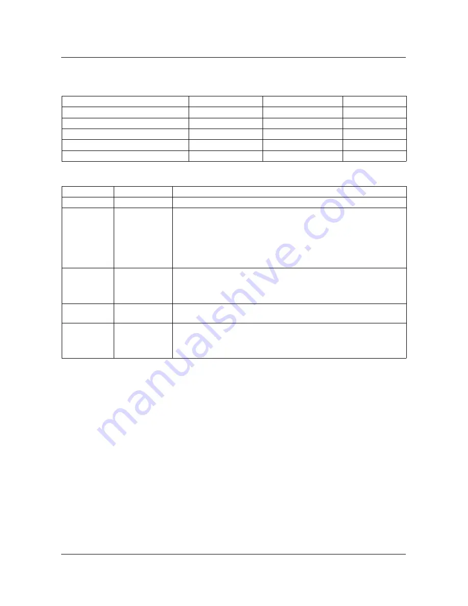
Absolute Maximum Ratings
(Ta=25
°
C unless otherwise specified)
PIN Definitions
Parameter
Symbol
Value
Unit
Maximum Vstr Pin Voltage
V
str,max
700
V
Maximum Supply Voltage
V
CC,MAX
10
V
Input Voltage Range
V
FB
−
0.3 to V
SD
V
Operating Ambient Temperature
T
A
−
25 to +85
°
C
Storage Temperature Range
T
STG
−
55 to +150
°
C
Pin Number
Pin Name
Pin Function Description
1, 2, 3
GND
These pins are the control ground and the SenseFET Source.
4
Vfb
This pin is the inverting input of the PWM comparator. It operates normally
between 0.5V and 2.5V. It has a 0.25mA current source connected internally
and a capacitor and opto coupler connected externally. A feedback voltage
of 3V to 4V triggers overload protection (OLP). There is a time delay due to
the 5uA current source, which prevents false triggering under transient
conditions but still allows the protection mechanism to operate under true
overload conditions.
5
Vcc
This is the positive supply voltage input. During start up, current is supplied
to this pin from Pin 8 via an internal switch. When Vcc reaches the UVLO
upper threshold (7V), the internal switch start-up switch (Vstr) opens and
power is supplied from auxiliary transformer winding.
7
Drain
This pin is designed to directly drive the converter transformer and is
capable of switching a maximum of 700V.
8
Vstr
This pin connects directly to the rectified AC line voltage source. At start up
the internal switch supplies internal bias and charges an external capacitor
that connects from the Vcc pin to ground. once this reaches 7V, the internal
current source is disabled.