background image

ESMT


 F25L04PA 

(2D)


Elite Semiconductor Memory Technology Inc.


Publication D

ateAug.

 2012


Revision:


1.4


3/33


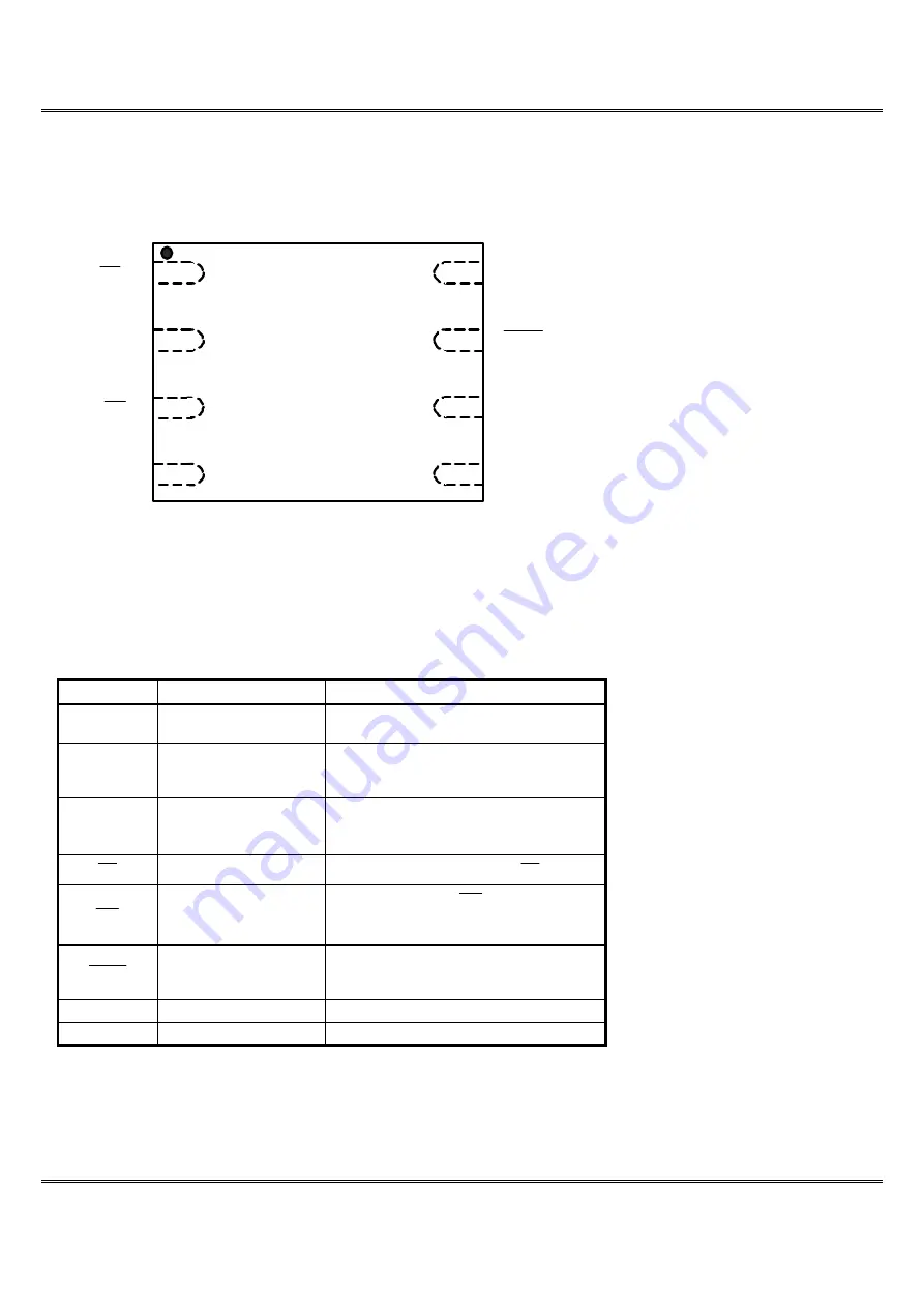
8- Contact WSON 

(WSON 8C, 6mmX5mm Body, 1.27mm Contact Pitch) 


PIN DESCRIPTION   


Symbol Pin 

Name 

Functions 

SCK Serial 

Clock 

To provide the timing for serial input and 
output operations 

SI 

Serial Data Input 

To transfer commands, addresses or data 
serially into the device. 
Data is latched on the rising edge of SCK.

SO 

Serial Data Output 

To transfer data serially out of the device. 
Data is shifted out on the falling edge of 
SCK. 

CE  

Chip Enable 

To activate the device when  CE  is low. 

WP  

Write Protect 

The Write Protect ( WP ) pin is used to 
enable/disable BPL bit in the status 
register. 

HOLD  

Hold 

To temporality stop serial communication 
with SPI flash memory without resetting 
the device. 

VDD 

Power Supply 

To provide power. 

VSS Ground 


1

2

3

4

8

7

6

5

CE

SO

WP

VSS

VDD

HOLD

SCK

SI

Summary of Contents for F25L04PA Series

Page 1: ...SOIC 150 mil Pb free F25L04PA 50PAG2D 50MHz F25L04PA 86PAG2D 86MHz F25L04PA 100PAG2D 100MHz 8 lead SOIC 200 mil Pb free F25L04PA 50HG2D 50MHz F25L04PA 86HG2D 86MHz F25L04PA 100HG2D 100MHz 8 contact WSON 6x5 mm Pb free GENERAL DESCRIPTION The F25L04PA is a 4Megabit 3V only CMOS Serial Flash memory device The device supports the standard Serial Peripheral Interface SPI and a Dual SPI ESMT s memory d...

Page 2: ...miconductor Memory Technology Inc Publication Date Aug 2012 Revision 1 4 2 33 PIN CONFIGURATIONS 8 Lead SOIC SOIC 8L 150mil Body 1 27mm Pin Pitch SOIC 8L 208mil Body 1 27mm Pin Pitch 1 8 2 7 3 6 4 5 VDD HOLD SCK SI CE SO WP VSS ...

Page 3: ... or data serially into the device Data is latched on the rising edge of SCK SO Serial Data Output To transfer data serially out of the device Data is shifted out on the falling edge of SCK CE Chip Enable To activate the device when CE is low WP Write Protect The Write Protect WP pin is used to enable disable BPL bit in the status register HOLD Hold To temporality stop serial communication with SPI...

Page 4: ...ductor Memory Technology Inc Publication Date Aug 2012 Revision 1 4 4 33 FUNCTIONAL BLOCK DIAGRAM Address Buffers and Latches X Decoder Flash Y Decoder I O Butters and Data Latches Serial Interface Control Logic CE SCK SI WP SO HOLD ...

Page 5: ...27 4KB 07F000H 07FFFFH 7 112 4KB 070000H 070FFFH 1 1 1 111 4KB 06F000H 06FFFFH 6 96 4KB 060000H 060FFFH 1 1 0 95 4KB 05F000H 05FFFFH 5 80 4KB 050000H 050FFFH 1 0 1 79 4KB 04F000H 04FFFFH 4 64 4KB 040000H 040FFFH 1 0 0 63 4KB 03F000H 03FFFFH 3 48 4KB 030000H 030FFFH 0 1 1 47 4KB 02F000H 02FFFFH 2 32 4KB 020000H 020FFFH 0 1 0 31 4KB 01F000H 01FFFFH 1 16 4KB 010000H 010FFFH 0 0 1 15 4KB 00F000H 00FFF...

Page 6: ... BP0 and TB are read writable 0 R W Note 1 Only BP0 BP1 BP2 TB and BPL are writable 2 BP0 BP1 BP2 TB and BPL are non volatile 3 All area are unprotected at power on BP2 BP1 BP0 0 WRITE ENABLE LATCH WEL The Write Enable Latch bit indicates the status of the internal memory Write Enable Latch If this bit is set to 1 it indicates the device is Write enabled If the bit is set to 0 reset it indicates t...

Page 7: ...00000H 06FFFFH All Blocks X 1 0 0 Block 0 7 000000H 07FFFFH All Blocks X 1 1 1 Block 0 7 000000H 07FFFFH Block Protection BP2 BP1 BP0 The Block Protection BP2 BP1 BP0 bits define the size of the memory area as defined in Table 3 to be software protected against any memory Write Program or Erase operations The Write Status Register WRSR instruction is used to program the BP2 BP1 BP0 bits as long as...

Page 8: ...E is driven active high during a Hold condition it resets the internal logic of the device As long as HOLD signal is low the memory remains in the Hold condition To resume communication with the device HOLD must be driven active high and CE must be driven active low See Figure 22 for Hold timing A ctive H o ld A cti ve H old A ctive H O L D S C K Figure 1 HOLD Condition Waveform WRITE PROTECTION T...

Page 9: ... A15 A8 Hi Z A7 A0 Hi Z X X X DOUT0 X cont Fast Read Dual Output 11 12 50MHz 86 MHz 3BH A23 A16 A15 A8 A7 A0 X DOUT0 1 cont Sector Erase 4 4K Byte 20H Hi Z A23 A16 Hi Z A15 A8 Hi Z A7 A0 Hi Z Block Erase 4 64K Byte D8H Hi Z A23 A16 Hi Z A15 A8 Hi Z A7 A0 Hi Z Chip Erase 60H C7H Hi Z Page Program PP 02H Hi Z A23 A16 Hi Z A15 A8 Hi Z A7 A0 Hi Z DIN0 Hi Z DIN1 Hi Z Up to 256 bytes Hi Z Read Status Re...

Page 10: ... very next bus cycle after the WREN instruction to make both instructions effective WREN can enable WRSR user just need to execute it A successful WRSR can reset WREN 10 The Manufacture ID and Device ID output will repeat continuously until CE terminates the instruction 11 Dual commands use bidirectional IO pins DOUT and cont are serial data out others are serial data in 12 Dual output data IO0 D6...

Page 11: ... Read instruction is initiated by executing an 8 bit command 03H followed by address bits A23 A0 CE must remain active low for the duration of the Read cycle See Figure 2 for the Read sequence Figure 2 Read Sequence Fast Read 50 MHz 100 MHz The Fast Read instruction supporting up to 100 MHz is initiated by executing an 8 bit command 0BH followed by address bits A23 A0 and a dummy byte CE must rema...

Page 12: ...red from the device at twice the rate of standard SPI devices This instruction is for quickly downloading code from Flash to RAM upon power up or for applications that cache code segments to RAM for execution The Fast Read Dual Output instruction is initiated by executing an 8 bit command 3BH followed by address bits A23 A0 and a dummy byte CE must remain active low for the duration of the Fast Re...

Page 13: ...page from the address whose 8 least significant bits A7 A0 are all zero If more than 256 bytes Data are sent to the device previously latched data are discarded and the last 256 bytes Data are guaranteed to be programmed correctly within the same page If less than 256 bytes Data are sent to device they are correctly programmed at the requested addresses without having any effects on the other byte...

Page 14: ... timed Block Erase cycle See Figure 8 for the Block Erase sequence Figure 8 64K byte Block Erase Sequence 4K Byte Sector Erase The Sector Erase instruction clears all bits in the selected sector to FFH A Sector Erase instruction applied to a protected memory area will be ignored Prior to any Write operation the Write Enable WREN instruction must be executed CE must remain active low for the durati...

Page 15: ...e internal self timed Chip Erase cycle See Figure 10 for the Chip Erase sequence Figure 10 Chip Erase Sequence Read Status Register RDSR The Read Status Register RDSR instruction allows reading of the status register The status register may be read at any time even during a Write Program Erase operation When a Write operation is in progress the Busy bit may be checked before sending any new comman...

Page 16: ...to any Write Program Erase operation CE must be driven high before the WREN instruction is executed Figure 12 Write Enable WREN Sequence Write Disable WRDI The Write Disable WRDI instruction resets the Write Enable Latch bit to 0 disabling any new Write operations from occurring CE must be driven high before the WRDI instruction is executed Figure 13 Write Disable WRDI Sequence CE SCK SI 0 1 2 3 4...

Page 17: ...ster but cannot be reset from 1 to 0 When WP is high the lock down function of the BPL bit is disabled and the BPL TB BP0 BP1 and BP2 bits in the status register can all be changed As long as BPL bit is set to 0 or WP pin is driven high VIH prior to the low to high transition of the CE pin at the end of the WRSR instruction the bits in the status register can all be altered by the WRSR instruction...

Page 18: ...on The instruction can be used to release the device from the deep power down status This instruction is initiated by driving CE low and executing an 8 bit command ABH and then drive CE high See Figure 16 for RDP instruction Release from the deep power down will take the duration of TRES1 before the device will resume normal operation and other instructions are accepted CE must remain high during ...

Page 19: ...Sequence Table 6 Electronic Signature Data Command Electronic Signature Data RES 12H SCK 0 1 2 3 4 5 6 7 MODE3 MODE0 SI CE Standby Current TRES1 MSB AB Deep Power Down Current ISB2 SO HIGH IMPEDANCE SCK 0 1 2 3 4 5 6 7 8 9 MODE3 MODE0 SI CE Standby Current TRES2 MSB AB Deep Power Down Current ISB2 SO HIGH IMPEDANCE SS 30 31 32 33 34 35 36 37 38 SS Electronic Signature Data Out SS MSB 3 Dummy Bytes...

Page 20: ...T Byte2 30H identifies the memory type as SPI Flash Byte3 13H identifies the device as F25L04PA The instruction sequence is shown in Figure 18 The JEDEC Read ID instruction is terminated by a low to high transition on CE at any time during data output If no other command is issued after executing the JEDEC Read ID instruction issue a 00H NOP command before going into Standby Mode CE VIH Figure 18 ...

Page 21: ... device ID is located in address 000001H Once the device is in Read ID mode the manufacturer s and device ID output data toggles between address 000000H and 000001H until terminated by a low to high transition on CE Figure 19 Read ID Sequence Table 8 Product ID Data Address Byte1 Byte2 8CH 12H 000000H Manufacturer s ID Device ID ESMT F25L04PA 12H 8CH 000001H Device ID ESMT F25L04PA Manufacturer s ...

Page 22: ...than one output shorted at a time AC CONDITIONS OF TEST OPERATING RANGE Parameter Symbol Value Unit Operating Supply Voltage VDD 2 3 3 6 V Ambient Operating Temperature TA 40 85 Table 9 DC OPERATING CHARACTERISTICS Limits Symbol Parameter Min Max Unit Test Condition Standard 8 IDDR1 Read Current 33 MHz Dual 10 mA CE 0 1 VDD 0 9 VDD SO open Standard 12 IDDR2 Read Current 50MHz Dual 14 mA CE 0 1 VDD...

Page 23: ...mbol Parameter Min Max Min Max Min Max Min Max Unit FCLK Serial Clock Frequency 33 50 86 100 MHz TSCKH 2 Serial Clock High Time 13 9 5 4 ns TSCKL 2 Serial Clock Low Time 13 9 5 4 ns TCLCH Clock Rise Time Slew Rate 0 1 0 1 0 1 0 1 V ns TCHCL Clock Fall Time Slew Rate 0 1 0 1 0 1 0 1 V ns TCES 1 CE Active Setup Time 5 5 5 5 ns TCEH 1 CE Active Hold Time 5 5 5 5 ns TCHS 1 CE Not Active Setup Time 5 5...

Page 24: ... Mode 3 3 3 3 us TRES1 3 CE High to Standby Mode for DP 3 3 3 3 us TRES2 3 CE High to Standby Mode for RES 1 8 1 8 1 8 1 8 us Note 1 Relative to SCK 2 TSCKH TSCKL must be less than or equal to 1 FCLK 3 Value guaranteed by characterization not 100 tested in production 4 Only applicable as a constraint for a Write status Register instruction when Block Protection Look BPL bit is set at 1 ERASE AND P...

Page 25: ...ESMT F25L04PA 2D Elite Semiconductor Memory Technology Inc Publication Date Aug 2012 Revision 1 4 25 33 Figure 20 Serial Input Timing Diagram Figure 21 Serial Output Timing Diagram ...

Page 26: ... Semiconductor Memory Technology Inc Publication Date Aug 2012 Revision 1 4 26 33 Figure 22 HOLD Timing Diagram Figure 23 Write Protect setup and hold timing during WRSR when BPL 1 CE SCK SI HIGH IMPENANCE SO TWHSL TSHWL WP ...

Page 27: ...is allowed Device is fully accessible Program Erase and Write command is ignored CE must track VCC Figure 24 Power Up Timing Diagram Table 12 Power Up Timing and VWI Threshold Parameter Symbol Min Max Unit VCC min to CE low TVSL 10 us Time Delay before Write instruction TPUW 1 10 ms Write Inhibit Threshold Voltage VWI 1 2 V Note These parameters are characterized only ...

Page 28: ...on Date Aug 2012 Revision 1 4 28 33 Figure 25 AC Input Output Reference Waveforms Figure 26 A Teat Load Example Input timing reference level Output timing reference level 0 8VCC 0 2VCC 0 7VCC 0 3VCC 0 5VCC AC Measurement Level Note Input pulse rise and fall time are 5ns ...

Page 29: ...ch Symbol Min Norm Max Min Norm Max Symbol Min Norm Max Min Norm Max A 1 35 1 60 1 75 0 053 0 063 0 069 D 4 80 4 90 5 00 0 189 0 193 0 197 A1 0 10 0 15 0 25 0 004 0 006 0 010 E 3 80 3 90 4 00 0 150 0 154 0 157 A2 1 25 1 45 1 55 0 049 0 057 0 061 L 0 40 0 66 0 86 0 016 0 026 0 034 b 0 33 0 406 0 51 0 013 0 016 0 020 e 1 27 BSC 0 050 BSC c 0 19 0 203 0 25 0 0075 0 008 0 010 L1 1 00 1 05 1 10 0 039 0...

Page 30: ...ension in inch Symbol Min Norm Max Min Norm Max Symbol Min Norm Max Min Norm Max A 2 16 0 085 E 7 70 7 90 8 10 0 303 0 311 0 319 A1 0 05 0 15 0 25 0 002 0 006 0 010 E1 5 18 5 28 5 38 0 204 0 208 0 212 A2 1 70 1 80 1 91 0 067 0 071 0 075 L 0 50 0 65 0 80 0 020 0 026 0 032 b 0 36 0 41 0 51 0 014 0 016 0 020 e 1 27 BSC 0 050 BSC c 0 19 0 20 0 25 0 007 0 008 0 010 L1 1 27 1 37 1 47 0 050 0 054 0 058 D...

Page 31: ...n Norm Max A 0 70 0 75 0 80 0 028 0 030 0 031 A1 0 00 0 02 0 05 0 000 0 001 0 002 b 0 35 0 40 0 45 0 014 0 016 0 018 D 5 90 6 00 6 10 0 232 0 236 0 240 D2 2 50 2 60 2 70 0 098 0 102 0 106 E 4 90 5 00 5 10 0 193 0 197 0 201 E2 2 10 2 20 2 30 0 083 0 087 0 091 e 1 27 BSC 0 050 BSC L 0 55 0 60 0 65 0 022 0 024 0 026 Controlling dimension millimeter PIN 1 PIN 1 D E e A A1 b L A B DETAIL B DETAIL A E2 ...

Page 32: ...e setting for all blocks in Block Protection Table 4 Modify the specification of ISB2 TSE max and TBE max 1 1 2011 03 03 1 Add device can support 100MHz in signal output Max load capacitance is 15pF 2 Modify WSON 6x5mm dimension D2 2 5 min 2 60 norm 2 70 max and E2 2 10 min 2 20 norm 2 30 max 1 2 2011 05 13 Modify the specification of ISB1 1 3 2012 04 18 Correct the figure of WSON packing dimensio...

Page 33: ...or other intellectual property rights of third parties which may result from its use No license either express implied or otherwise is granted under any patents copyrights or other intellectual property rights of ESMT or others Any semiconductor devices may have inherently a certain rate of failure To minimize risks associated with customer s application adequate design and operating safeguards ag...

Reviews: