background image

Page 24 total 3 


Chapter 4

BIOS 


4.1 BIOS introduction 

4.1.1  BIOS Description 

BIOS

Basic Input an Output System

),

Through the CMOS chip on the motherboard, the set 

parameters of the system's various hardware devices are recorded. The BIOS contains a BIOS 
setup program for users to set their own system parameters as needed to make the motherboard 
work properly or perform specific functions. The relevant settings (except date and time) modified by 
the BIOS Setup program are stored in the flash memory in the system, and the power needed to 
remember the CMOS data is supplied by the battery on the motherboard, so that when the system is 
powered off, the information will not be lost, and the system will be able to read the set data when 
the power is switched on again. 
Since the settings interface of our different products will be slightly different, the following screen for 
your reference, it is possible that you are currently using the BIOS setup program is not exactly the 
same. 

4.1.2  Access to BIOS system methods 

1. Power on the system or restart the system, 
2. After powering on, when the screen self-test information appears, when the middle of the screen 
appears "Press <DEL> to enter setup,<f11>to Popup menu" prompt, press the <Del> key to enter 
the BIOS 

4.1.3  In the BOIS interface, the key functions are as follows; 

→←


Select a menu 

↑↓


Select 

-  Enter


-  +/- : change value 

-  F1 

help 

-  F2 


Discard this modification and go back to the last set value. 

-  F9 


Restoring factory defaults 

-  F10 


Save changes and exit 
Summary of Contents for LUMIA2MINIA1350

Page 1: ...Page 1 total 38 Industrial grade box PC LUMIA2MINIA1350 User manual Connect Ideas Shape solutions ...

Page 2: ...ttings JBAT1 12 Chapter 3 PIN IO Interface 13 3 1 Front interface layout 13 3 2 Back interface layout 14 3 3 PIN Distribution 15 3 3 1 VGA1 VGA2 15 3 3 2 AUDIO1 15 3 3 3 COM1 15 3 3 4 LVDS1 and EDP alternatively 16 3 3 5 LCD_12_5_3V 17 3 3 6 LVDS_P1 和 EDP 17 3 3 7 JP1 18 3 3 8 CPU_FAN1 SYS_FAN1 18 3 3 9 U17 18 3 3 10 RTC1 18 3 3 11 BAT1 18 3 3 12 GPIO1 19 3 3 13 FP1 19 3 3 14 JP2 20 3 4 Interface ...

Page 3: ...IOS system methods 27 4 1 3 In the BOIS interface the key functions are as follows 27 4 1 4 Precautions 28 4 2 BIOS Basic functionality settings 28 4 2 1 Main 28 4 2 2 Advanced 29 4 2 3 Chipset 30 4 2 4 Security 31 4 2 5 Boot 32 4 2 6 Save Exit 33 Appendix 34 Appendix I Glossary 34 Appendix II Common Fault Analysis and Resolution 37 ...

Page 4: ...r 1 reset button 1 Power Indicator 1 HDD indicator support 255 level watchdog This motherboard can be worked stably in the temperature 20 60 degrees 0 to 90 relative humidity non condensation condition to meet the needs of various applications of industrial grade products The product combines the advantages of stable and reliable industrial grade product performance and intelligent digital multime...

Page 5: ...Page 5 total 3 1 2 Main board Picture ...

Page 6: ...rk Controller 2 Intel I211gigabit Ethernet RJ45 Port Audio Controller Realtek HD ALC662 audio decoder Left Right channel Microphone Super I O Controller ITE8613 Hardware monitor Watch dog timer 0 255s Provide watch dog routines Cooler Aluminum FAN radiator can choose fanless Input output interface USB 2 USB2 0 2 USB3 0 maximum support 5V 1A Series port 1 RS 232 RJ45 interface GPIO 8bit providing r...

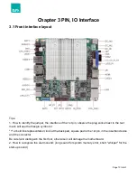
Page 7: ... is the front interface location and dimension sits of the board Care must be taken during the installation of the device Some parts if installed incorrectly will not work properly Tips Be sure to select the right screws and use the correct installation method as this may damage the motherboard ...

Page 8: ...PU RAM etc 3 Before the integrated circuit components are installed the components should be placed in an anti static pad or anti static bag 4 Plug in the power supply after confirming that the switch to the power supply is in the open position 2 2 2 Memory installation There are two things to note when installing a memory bar 1 When installing align the notch of the memory strip with the notch of...

Page 9: ...y settings system settings The steps 1 Turn off the computer disconnect the power 2 turn off the computer disconnect the power 2 use the jumper cap to short JBAT1 pin 1 and 2 short 5 to 6 seconds and then restore 3 Start and press the Delete key in the keyboard to enter the BIOS interface 4 Enter the BIOS interface by pressing the F9 key return overload the optimal default value 5 Press F10 to sav...

Page 10: ...ext to the text mark will use the triangle symbol or 1 or bold line representation look at the back pad square pad is the 1st pin in the insertion device and the connector Be careful to distinguish the first foot otherwise it will damage the motherboard 2 How to recognize the alarm sound long sound for system memory error short whisper for the start up sound ...

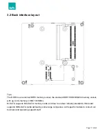
Page 11: ...he standard DDR3 SODIMM204 memory socket with up to 4G memory 1066 1333MHz M SATA supports Mini SATA memory cards and due to unclear industry standards this board supports MINI SATA cards defined by some large companies with specific models to consult our business and operating support staff ...

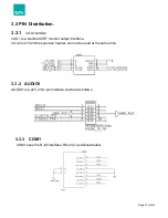
Page 12: ... VGA2 VAG1 is a standard CRT monitor output interface VGA2 is 2 5 2mm expansion header can not be used at the same time 3 3 2 AUDIO1 AUDIO1 is a 2x5 2mm pin interface defined as follows 3 3 3 COM1 COM1 uses the RJ45 interface RS 232 as defined below ...

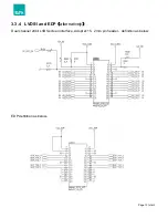
Page 13: ...Page 13 total 3 3 3 4 LVDS1 and EDP alternatively Dual channel 24bit LVDS screen interface Adopt 2x15 2mm pin header definition as below EDP definition as below ...

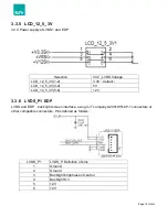
Page 14: ... default LCD_12_5_3V 3 4 5V LCD_12_5_3V 5 6 12V 3 3 6 LVDS_P1 EDP LVDS and EDP back light screen interface using CJT company A2001WR 6P 1 connectors or other compatible connectors Pins defined as follows LVDS_P1 LVDS_P Definition of pins 1 Ground 2 Ground 3 Backlight brightness of control 4 Backlight On 5 12V 6 12V ...

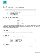
Page 15: ...onal speed adjust automatically The maximum voltage equal to the input power voltage Please choose a suitable fan when the input voltage is higher than input power SYS fan does not support adjust automatically 3 3 9 U17 The on board EMMC high speed memory chip 32 64 128G capacity is available 3 3 10 RTC1 RTC1 is the reset jumper of RTC adopt 1x2 2mm PIN header RTC1 Function declare Close Clear RTC...

Page 16: ...erface 2x5 2mm pin header integrated HDD_LED PWR_LED Power on switch Reset switch SPEAKER function The pins are defined as follows F_PANEL1 Pin definition 1 3 Positive Negative signal pin of HDD Read Write indicator 2 4 Positive Negative signal pin of Power indicator 5 7 Positive Negative signal pin of motherboard reset signal 6 8 Positive Negative signal pin of Power on off 9 10 Standby interface...

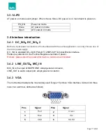
Page 17: ... DC _IN3 is standard DC JACK Ports DT 126RP 02P Terminal Blocks interface Please pay attention to the Positive Negative electrode of power Remark please input the power after devices cables are all installed 3 4 2 LINE_OUT2 MIC_IN MIC_IN is the input of MICPHONE Adopt general connector LINE_OUT is audio output port adopt general connector 3 4 3 VGA The motherboard adopts the most widely used D typ...

Page 18: ...image transmission of a special digital interface which can transmit audio and audio signals at the same time the maximum data transmission speed of 5Gbps defined as follows Pins Signal Pins Signal 1 TMDS Data2 2 TMDS Data2 Shield 3 TMDS Data2 4 TMDS Data1 5 TMDS Data1 Shield 6 TMDS Data1 7 TMDS Data0 8 TMDS Data0 Shield 9 TMDS Data0 10 TMDS Clock 11 TMDS Clock Shield 12 TMDS Clock 13 CEC 14 Reser...

Page 19: ...out shutting down the computer as defined below Pins USB 3 0 USB 2 0 1 5V_USB 5V_USB 2 USB_DATA USB_DATA 3 USB_DATA USB_DATA 4 GND GND 5 USB_SSRX 6 USB_SSRX 7 GND 8 USB_SSTX 9 USB_SSTX 3 4 6 SIM2 This motherboard adopts Nano SIM drawer type six legged card holder defined as follows Pins Signal Pins Signal 1 VCC 2 RST 3 CLK 4 GND1 5 GND0 6 VPP 7 I_O ...

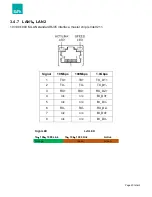
Page 20: ... interface master chip is Intel I211 Signal 10Mbps 100Mbps 1 0Gbps 1 TX TX TX_D1 2 TX TX TX_D1 3 RX RX RX_D2 4 n c n c BI_D3 5 n c n c BI_D3 6 RX RX RX_D2 7 n c n c BI_D4 8 n c n c BI_D4 Right LED Left LED 10 100 1000 Link 10 100 1000 Link Active Orange Green Green ...

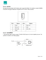
Page 21: ...ts 600MB s bandwidth throughput Backward compatible with The SATA 3 Gb s interface Pins Signal Pins Signal 1 GND 2 SATA_TX 3 SATA_TX 4 GND 5 SATA_RX 6 SATA_RX 7 GND 3 4 9 SATAPWR 1 SATA device power interface using CJT A2501WV 2P devices or other compatible devices The definition is similar to the following figure ...

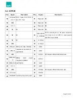
Page 22: ...output for 3 3 V aux or 3 3 V PCI 1 1 was reserved and PIC1 2 was GND 42 NC NC 41 3 3Vaux 40 GND 39 3 3Vaux 38 USB_D USB serial data interface compliant to the USB 2 0 specification 37 GND 36 USB_D 35 GND 34 GND 33 PETp0 PCI Express differential transmit pair 32 SMB_DAT A SMBus data signal compliant to SMBus specification 31 PETn0 30 SMB_CLK 29 GND 28 1 5 V 27 GND 26 GND 25 PERp0 PCI Express diffe...

Page 23: ...C NC 15 GND 14 NC NC 13 REFCLK 12 NC NC 11 REFCLK 10 NC NC 9 GND 8 NC NC 7 CLKREQ Reference clock request signal 6 V 5 NC NC 4 GND 3 NC NC 2 3 3Vaux 3 3 V PCI 1 1 was 3 3 V PCI 1 2 was 3 3 V aux 1 WAKE Open drain active low signal This signal is used to request that the system return from a sleep suspended state to service a function initiated wake event 3 3 V aux was suspend power with power out ...

Page 24: ...ed off the information will not be lost and the system will be able to read the set data when the power is switched on again Since the settings interface of our different products will be slightly different the following screen for your reference it is possible that you are currently using the BIOS setup program is not exactly the same 4 1 2 Access to BIOS system methods 1 Power on the system or r...

Page 25: ...uses the power cannot be turned on please restore the factory mode 4 2 BIOS Basic functionality settings 4 2 1 Main System Date Set the system date In month day year format The range is Mon Month Jan Dec Date Day 01 31 Year Year up to 2099 System Time set system time Expressed in hour minute second format It is set up in the range Hour 00 23 Minute min 00 59 Second S 00 59 The black font section i...

Page 26: ...713 Super IO Configuration COM port watchdog GPIO information and control options Hardware Monitor Fan automatic speed adjustment CPU temperature display and other related settings Serial Port Console Redirection serial console redirects CPU Configuration Network Stack Configuration PXE startup settings CSM Configuration the system selects the relevant settings such as UEFI ...

Page 27: ...idge Graphics card related settings memory information displayed South Bridge power on boot serial port IRQ mode system selection and other related settings Uncore Configuration SATA Configuration PCI Express Configuration SCC Configuration ...

Page 28: ...assword User Password The prompt line is used to set the normal user password Tip The minimum length of the password is 3 digits and the maximum length is 20 bits If you forget your password the short pin RTC1 5 seconds or the BAT1 is unplugged and the positive and negative short 5 seconds clears the password ...

Page 29: ... time settings Quiet Boot Quick Start Settings Boot Option Priorities Boot Option 1 first boot item settings Boot Option 2 second startup item settings Hard Drive BBS Priorities new hard drive start option settings USB Drive BBS Priorities new USB boot option settings ...

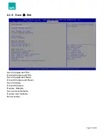
Page 30: ... 4 2 6 Save Exit Save Changes and Exit Discard Changes and Exit Save Changes and Reset Discard Changes and Reset Save Changes Discard Changes Restore Defaults Save as User Defaults Restore User Defaults Boot Override ...

Page 31: ...ing to is usually a local line inside the CPU and the main memory element Chipset an integrated chip designed to perform one or more related functions We are referring to a system level chipset made up of South bridge and Northbridge which determines the architecture and main functions of the motherboard AHCI Standard control interface for serial ATA supported by Microsoft Windows XP above SP1 and...

Page 32: ...mmonly used today LAN The lan area interface A computer network consisting of interconnected computers in a small area usually in an enterprise or building Lan area networks are generally composed of servers workstations and some communication links a terminal that can access data and devices through wires and many users can share expensive equipment and resources Led A light emitting diode a semi...

Page 33: ...ch as modems Usb Universal serial bus A hardware interface suitable for low speed peripherals generally used to connect keyboards mice etc A PC can connect up to 127 USB devices providing a 12Mbit s transmission bandwidth and USB supports hot swap and multi data capabilities which allow USB devices to be plugged into when the system is working and the system can automatically identify and allow th...

Page 34: ...ception of the card is normal VGA does not display after power on 1 Check if the monitor is turned on 2 Check that the power cord is properly connected to the monitor and system unit 3 Check that the display cable is properly connected to the system unit and monitor 4 See if the display brightness control is set to a dark state and you can increase the brightness through the brightness control For...

Page 35: ...lease make sure that the CPU cooling fan is turning normally 4 Re install the OS System auto reboot 1 Please make sure that the CPU cooling fan is turning properly 2 Please confirm that the reset button is triggered by mistake 3 Please use antivirus software to confirm that the system is infected with a virus 4 Please make sure the memory bar and the external card are loose 5 Please confirm that t...

Page 36: ...Page 36 total 3 Connect Ideas Shape solutions ...

Reviews: