EDM01-14 DAG 3.6D Card User Guide
©2005
3
Version 10: May 2006
1.3 DAG 3.6D Card Architecture
, continued
Description
Serial PDH data is received by the DAG 3.6D card co-axial interfaces, and
fed through a Signal Equaliser into the upper of two Xilinx FPGAs.
This FPGA contains a PDH framer and the DUCK timestamp engine. The
close association of these two components means that packets or cells can
be time-stamped very accurately.
Figure
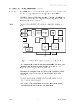
Figure 1-2 shows the DAG 3.6D card major components and process
flow.
Figure 1-2. DAG 3.6D Card Major Components and Process Flow.
Time stamped packet or cell records are stored in a FIFO. The DAG 3.6D
can demap either ADM (ATM Direct Mapped) ATM cells, or PLCP
(Payload Layer Convergence Protocol) ATM cells.
Records are then transferred from the FIFO into the lower FPGA, which
has interfaces to the PCI bus and to the bus of the local StrongARM
processor.
The entire record is made available to the StrongARM processor in a
series of memory-mapped registers.
Code running on the StrongARM is then used to decide if the record
should be written to host PC memory over the PCI bus.
Summary of Contents for DAG 3.6D
Page 1: ......
Page 5: ...EDM01 14 DAG 3 6D Card User Guide 2005 ii Version 10 May 2006...
Page 21: ...EDM01 14 DAG 3 6D Card User Guide 2005 16 Version 10 May 2006...
Page 22: ...EDM01 14 DAG 3 6D Card User Guide 2005 17 Version 10 May 2006...
Page 26: ...EDM01 14 DAG 3 6D Card User Guide 2005 21 Version 10 May 2006...
Page 34: ...EDM01 14 DAG 3 6D Card User Guide 2005 29 Version 10 May 2006...


